Tag Archives: hardware

An update on Fitbit

Last year, we announced that Google entered into an agreement to acquire Fitbit to help spur innovation in wearable devices and build products that help people lead healthier lives. As we continue to work with regulators to answer their questions, we wanted to share more about how we believe this deal will increase choice, and create engaging products and helpful experiences for consumers.

There's vibrant competition when it comes to smartwatches and fitness trackers, with Apple, Samsung, Garmin, Fossil, Huawei, Xiaomi and many others offering numerous products at a range of prices. We don’t currently make or sell wearable devices like these today. We believe the combination of Google and Fitbit's hardware efforts will increase competition in the sector, making the next generation of devices better and more affordable. 

This deal is about devices, not data. We’ve been clear from the beginning that we will not use Fitbit health and wellness data for Google ads. We recently offered to make a legally binding commitment to the European Commission regarding our use of Fitbit data. As we do with all our products, we will give Fitbit users the choice to review, move or delete their data. And we’ll continue to support wide connectivity and interoperability across our and other companies’ products. 

We appreciate the opportunity to work with the European Commission on an approach that addresses consumers' expectations of their wearable devices. We’re confident that by working closely with Fitbit’s team of experts, and bringing together our experience in AI, software and hardware, we can build compelling devices for people around the world.

Enabling E-Textile Microinteractions: Gestures and Light through Helical Structures


Textiles have the potential to help technology blend into our everyday environments and objects by improving aesthetics, comfort, and ergonomics. Consumer devices have started to leverage these opportunities through fabric-covered smart speakers and braided headphone cords, while advances in materials and flexible electronics have enabled the incorporation of sensing and display into soft form factors, such as jackets, dresses, and blankets.
A scalable interactive E-textile architecture with embedded touch sensing, gesture recognition and visual feedback.
In “E-textile Microinteractions” (Proceedings of ACM CHI 2020), we bring interactivity to soft devices and demonstrate how machine learning (ML) combined with an interactive textile topology enables parallel use of discrete and continuous gestures. This work extends our previously introduced E-textile architecture (Proceedings of ACM UIST 2018). This research focuses on cords, due to their modular use as drawstrings in garments, and as wired connections for data and power across consumer devices. By exploiting techniques from textile braiding, we integrate both gesture sensing and visual feedback along the surface through a repeating matrix topology.

For insight into how this works, please see this video about E-textile microinteractions and this video about the E-textile architecture.
E-textile microinteractions combining continuous sensing with discrete motion and grasps.
The Helical Sensing Matrix (HSM)
Braiding generally refers to the diagonal interweaving of three or more material strands. While braids are traditionally used for aesthetics and structural integrity, they can also be used to enable new sensing and display capabilities.

Whereas cords can be made to detect basic touch gestures through capacitive sensing, we developed a helical sensing matrix (HSM) that enables a larger gesture space. The HSM is a braid consisting of electrically insulated conductive textile yarns and passive support yarns,where conductive yarns in opposite directions take the role of transmit and receive electrodes to enable mutual capacitive sensing. The capacitive coupling at their intersections is modulated by the user’s fingers, and these interactions can be sensed anywhere on the cord since the braided pattern repeats along the length.
Left: A Helical Sensing Matrix based on a 4×4 braid (8 conductive threads spiraled around the core). Magenta/cyan are conductive yarns, used as receive/transmit lines. Grey are passive yarns (cotton). Center: Flattened matrix, that illustrates the infinite number of 4×4 matrices (colored circles 0-F), which repeat along the length of the cord. Right: Yellow are fiber optic lines, which provide visual feedback.
Rotation Detection
A key insight is that the two axial columns in an HSM that share a common set of electrodes (and color in the diagram of the flattened matrix) are 180º opposite each other. Thus, pinching and rolling the cord activates a set of electrodes and allows us to track relative motion across these columns. Rotation detection identifies the current phase with respect to the set of time-varying sinusoidal signals that are offset by 90º. The braid allows the user to initiate rotation anywhere, and is scalable with a small set of electrodes.
Rotation is deduced from horizontal finger motion across the columns. The plots below show the relative capacitive signal strengths, which change with finger proximity.
Interaction Techniques and Design Guidelines
This e-textile architecture makes the cord touch-sensitive, but its softness and malleability limit suitable interactions compared to rigid touch surfaces. With the unique material in mind, our design guidelines emphasize:
  • Simple gestures. We design for short interactions where the user either makes a single discrete gesture or performs a continuous manipulation.

  • Closed-loop feedback. We want to help the user discover functionality and get continuous feedback on their actions. Where possible, we provide visual, tactile, and audio feedback integrated in the device.
Based on these principles, we leverage our e-textile architecture to enable interaction techniques based on our ability to sense proximity, area, contact time, roll and pressure.
Our e-textile enables interaction based on capacitive sensing of proximity, contact area, contact time, roll, and pressure.
The inclusion of fiber optic strands that can display color of varying intensity enable dynamic real-time feedback to the user.
Braided fiber optics strands create the illusion of directional motion.
Motion Gestures (Flicks and Slides) and Grasping Styles (Pinch, Grab, Pinch)
We conducted a gesture elicitation study, which showed opportunities for an expanded gesture set. Inspired by these results, we decided to investigate five motion gestures based on flicks and slides, along with single­-touch gestures (pinch, grab and pat).
Gesture elicitation study with imagined touch sensing.
We collected data from 12 new participants, which resulted in 864 gesture samples (12 participants performed eight gestures each, repeating nine times), each having 16 features linearly interpolated to 80 observations over time. Participants performed the eight gestures in their own style without feedback as we wanted to accommodate individual differences since the classification is highly dependent on user style (“contact”), preference (“how to pinch/grab”) and anatomy (e.g., hand size). Our pipeline was thus designed for user-dependent training to enable individual styles with differences across participants, such as the inconsistent use of clockwise/counterclockwise, overlap between temporal gestures (e.g., flick vs. flick and hold, and similar pinch and grab gestures.) For a user-independent system, we would need to address such differences, for example with stricter instructions for consistency, data from a larger population, and in more diverse settings. Real-time feedback during training will also help mitigate differences as the user learns to adjust their behavior.
Twelve participants (horizontal axis) performed 9 repetitions (animation) for the eight gestures (vertical axis). Each sub-image shows 16 overlaid feature vectors, interpolated to 80 observations over time.
We performed cross-validation for each user across the gestures by training on eight repetitions and testing on one, through nine permutations, and achieved a gesture recognition accuracy of ~94%. This result is encouraging, especially given the expressivity enabled by such a low-resolution sensor matrix (eight electrodes).

Notable here is that inherent relationships in the repeated sensing matrices are well-suited for machine learning classification. The ML classifier used in our research enables quick training with limited data, which makes a user-dependent interaction system reasonable. In our experience, training for a typical gesture takes less than 30s, which is comparable to the amount of time required to train a fingerprint sensor.

User-Independent, Continuous Twist: Quantifying Precision and Speed
The per-user trained gesture recognition enabled eight new discrete gestures. For continuous interactions, we also wanted to quantify how well user-independent, continuous twist performs for precision tasks. We compared our e-textile with two baselines, a capacitive multi-touch trackpad (“Scroll”) and the familiar headphone cord remote control (“Buttons”). We designed a lab study where the three devices controlled 1D movement in a targeting task.

We analysed three dependent variables for the 1800 trials, covering 12 participants and three techniques: time on task (milliseconds), total motion, and motion during end-of-trial. Participants also provided qualitative feedback through rankings and comments.

Our quantitative analysis suggests that our e-textile’s twisting is faster than existing headphone button controls and comparable in speed to a touch surface. Qualitative feedback also indicated a preference for e-textile interaction over headphone controls.
Left: Weighted average subjective feedback. We mapped the 7-point Likert scale to a score in the range [-3, 3] and multiplied by the number of times the technique received that rating, and computed an average for all the scores. Right: Mean completion times for target distances show that Buttons were consistently slower.
These results are particularly interesting given that our e-textile was more sensitive, compared to the rigid input devices. One explanation might be its expressiveness — users can twist quickly or slowly anywhere on the cord, and the actions are symmetric and reversible. Conventional buttons on headphones require users to find their location and change grips for actions, which adds a high cost to pressing the wrong button. We use a high-pass filter to limit accidental skin contact, but further work is needed to characterize robustness and evaluate long-term performance in actual contexts of use.

Gesture Prototypes: Headphones, Hoodie Drawstrings, and Speaker Cord
We developed different prototypes to demonstrate the capabilities of our e-textile architecture: e-textile USB-C headphones to control media playback on the phone, a hoodie drawstring to invisibly add music control to clothing, and an interactive cord for gesture controls of smart speakers.
Left: Tap = Play/Pause; Center: Double-tap = Next track; Right: Roll = Volume +/-
Interactive speaker cord for simultaneous use of continuous (twisting/rolling) and discrete gestures (pinch/pat) to control music playback.
Conclusions and Future Directions
We introduce an interactive e-textile architecture for embedded sensing and visual feedback, which can enable both precise small-scale and large-scale motion in a compact cord form factor. With this work, we hope to advance textile user interfaces and inspire the use of microinteractions for future wearable interfaces and smart fabrics, where eyes-free access and casual, compact and efficient input is beneficial. We hope that our e-textile will inspire others to augment physical objects with scalable techniques, while preserving industrial design and aesthetics.

Acknowledgements
This work is a collaboration across multiple teams at Google. Key contributors to the project include Alex Olwal, Thad Starner, Jon Moeller, Greg Priest-Dorman, Ben Carroll, and Gowa Mainini. We thank the Google ATAP Jacquard team for our collaboration, especially Shiho Fukuhara, Munehiko Sato, and Ivan Poupyrev. We thank Google Wearables, and Kenneth Albanowski and Karissa Sawyer, in particular. Finally, we would like to thank Mark Zarich for illustrations, Bryan Allen for videography, Frank Li for data processing, Mathieu Le Goc for valuable discussions, and Carolyn Priest-Dorman for textile advice.

Source: Google AI Blog


Chip Design with Deep Reinforcement Learning


The revolution of modern computing has been largely enabled by remarkable advances in computer systems and hardware. With the slowing of Moore’s Law and Dennard scaling, the world is moving toward specialized hardware to meet the exponentially growing demand for compute. However, today’s chips take years to design, resulting in the need to speculate about how to optimize the next generation of chips for the machine learning (ML) models of 2-5 years from now. Dramatically shortening the chip design cycle would allow hardware to adapt to the rapidly advancing field of ML. What if ML itself could provide the means to shorten the chip design cycle, creating a more integrated relationship between hardware and ML, with each fueling advances in the other?

In “Chip Placement with Deep Reinforcement Learning”, we pose chip placement as a reinforcement learning (RL) problem, where we train an agent (i.e, an RL policy) to optimize the quality of chip placements. Unlike prior methods, our approach has the ability to learn from past experience and improve over time. In particular, as we train over a greater number of chip blocks, our method becomes better at rapidly generating optimized placements for previously unseen chip blocks. Whereas existing baselines require human experts in the loop and take several weeks to generate, our method can generate placements in under six hours that outperform or match their manually designed counterparts. While we show that we can generate optimized placements for Google accelerator chips (TPUs), our methods are applicable to any kind of chip (ASIC).

The Chip Floorplanning Problem
A computer chip is divided into dozens of blocks, each of which is an individual module, such as a memory subsystem, compute unit, or control logic system. These blocks can be described by a netlist, a graph of circuit components, such as macros (memory components) and standard cells (logic gates like NAND, NOR, and XOR), all of which are connected by wires. Determining the layout of a chip block, a process called chip floorplanning, is one of the most complex and time-consuming stages of the chip design process and involves placing the netlist onto a chip canvas (a 2D grid), such that power, performance, and area (PPA) are minimized, while adhering to constraints on density and routing congestion. Despite decades of research on this topic, it is still necessary for human experts to iterate for weeks to produce solutions that meet multi-faceted design criteria. This problem’s complexity arises from the size of the netlist graph (millions to billions of nodes), the granularity of the grid onto which that graph must be placed, and the exorbitant cost of computing the true target metrics, which can take many hours (sometimes over a day) using industry-standard electronic design automation tools.

The Deep Reinforcement Learning Model
The input to our model is the chip netlist (node types and graph adjacency information), the ID of the current node to be placed, and some netlist metadata, such as the total number of wires, macros, and standard cell clusters. The netlist graph and the current node are passed through an edge-based graph neural network that we developed to encode the input state. This generates embeddings of the partially placed graph and the candidate node.
A graph neural network generates embeddings that are concatenated with the metadata embeddings to form the input to the policy and value networks.
The edge, macro and netlist metadata embeddings are then concatenated to form a single state embedding, which is passed to a feedforward neural network. The output of the feedforward network is a learned representation that captures the useful features and serves as input to the policy and value networks. The policy network generates a probability distribution over all possible grid cells onto which the current node could be placed.

In each iteration of training, the macros are sequentially placed by the RL agent, after which the standard cell clusters are placed by a force-directed method, which models the circuit as a system of springs to minimize wirelength. RL training is guided by a fast-but-approximate reward signal calculated for each of the agent’s chip placements using the weighted average of approximate wirelength (i.e., the half-perimeter wirelength, HPWL) and approximate congestion (the fraction of routing resources consumed by the placed netlist).
During each training iteration, the macros are placed by the policy one at a time and the standard cell clusters are placed by a force-directed method. The reward is calculated from the weighted combination of approximate wirelength and congestion.
Results
To our knowledge, this method is the first chip placement approach that has the ability to generalize, meaning that it can leverage what it has learned while placing previous netlists to generate better placements for new unseen netlists. We show that as we increase the number of chip netlists on which we perform pre-training (i.e., as our method becomes more experienced in placement optimization), our policy better generalizes to new netlists.

For example, the pre-trained policy organically identifies an arrangement that places the macros near the edges of the chip with a convex space in the center in which to place the standard cells. This results in lower wirelength between the macros and standard cells without introducing excessive routing congestion. In contrast, the policy trained from scratch starts with random placements and takes much longer to converge to a high-quality solution, rediscovering the need to leave an opening in the center of the chip canvas. This is demonstrated in the animation below.
Macro placements of Ariane, an open-source RISC-V processor, as training progresses. On the left, the policy is being trained from scratch, and on the right, a pre-trained policy is being fine-tuned for this chip. Each rectangle represents an individual macro placement. Notice how the cavity discovered by the from-scratch policy is already present from the outset in the pre-trained policy’s placement.
We observe that pre-training improves sample efficiency and placement quality. We compare the quality of placements generated using pre-trained policies to those generated by training the policy from scratch. To generate placements for previously unseen chip blocks, we use a zero-shot method, meaning that we simply use a pre-trained policy (with no fine-tuning) to place a new block, yielding a placement in less than a second. The results can be further improved by fine-tuning the policy on the new block. The policy trained from scratch takes much longer to converge, and even after 24 hours, its chip placements are worse than what the fine-tuned policy achieves after 12 hours.
Convergence plots for two policies on Ariane blocks. One is training from scratch and the other is finetuning a pre-trained policy.
The performance of our approach improves as we train on a larger dataset. We observed that as we increase the training set from two blocks to five blocks, and then to 20 blocks, the policy generates better placements, both at zero-shot and after being fine-tuned for the same training wall-clock time.
Training data size vs. fine-tuning performance.
The ability of our approach to learn from experience and improve over time unlocks new possibilities for chip designers. As the agent is exposed to a greater volume and variety of chips, it becomes both faster and better at generating optimized placements for new chip blocks. A fast, high-quality, automatic chip placement method could greatly accelerate chip design and enable co-optimization with earlier stages of the chip design process. Although we evaluate primarily on accelerator chips, our proposed method is broadly applicable to any chip placement problem. After all that hardware has done for machine learning, we believe that it is time for machine learning to return the favor.

Acknowledgements
This project was a collaboration between Google Research and Google Hardware and Architecture teams. We would like to thank our coauthors: Mustafa Yazgan, Joe Jiang, Ebrahim Songhori, Shen Wang, Young-Joon Lee, Eric Johnson, Omkar Pathak, Sungmin Bae, Azade Nazi, Jiwoo Pak, Andy Tong, Kavya Srinivasa, William Hang, Emre Tuncer, Anand Babu, Quoc Le, James Laudon, Roger Carpenter, Richard Ho, and Jeff Dean for their support and contributions to this work.

Source: Google AI Blog


uDepth: Real-time 3D Depth Sensing on the Pixel 4


The ability to determine 3D information about the scene, called depth sensing, is a valuable tool for developers and users alike. Depth sensing is a very active area of computer vision research with recent innovations ranging from applications like portrait mode and AR to fundamental sensing innovations such as transparent object detection. Typical RGB-based stereo depth sensing techniques can be computationally expensive, suffer in regions with low texture, and fail completely in extreme low light conditions.

Because the Face Unlock feature on Pixel 4 must work at high speed and in darkness, it called for a different approach. To this end, the front of the Pixel 4 contains a real-time infrared (IR) active stereo depth sensor, called uDepth. A key computer vision capability on the Pixel 4, this technology helps the authentication system identify the user while also protecting against spoof attacks. It also supports a number of novel capabilities, such as after-the-fact photo retouching, depth-based segmentation of a scene, background blur, portrait effects and 3D photos.

Recently, we provided access to uDepth as an API on Camera2, using the 
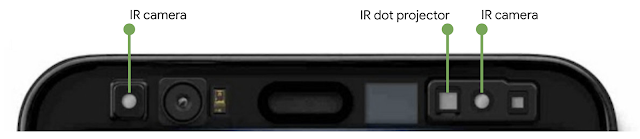
Pixel Neural Core, two IR cameras, and an IR pattern projector to provide time-synchronized depth frames (in DEPTH16) at 30Hz. The Google Camera App uses this API to bring improved depth capabilities to selfies taken on the Pixel 4. In this post, we explain broadly how uDepth works, elaborate on the underlying algorithms, and discuss applications with example results for the Pixel 4.

Overview of Stereo Depth Sensing
All stereo camera systems reconstruct depth using parallax. To observe this effect, look at an object, close one eye, then switch which eye is closed. The apparent position of the object will shift, with closer objects appearing to move more. uDepth is part of the family of dense local stereo matching techniques, which estimate parallax computationally for each pixel. These techniques evaluate a region surrounding each pixel in the image formed by one camera, and try to find a similar region in the corresponding image from the second camera. When calibrated properly, the reconstructions generated are metric, meaning that they express real physical distances.
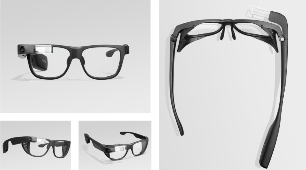
Pixel 4 front sensor setup, an example of an active stereo system.
To deal with textureless regions and cope with low-light conditions, we make use of an “active stereo” setup, which projects an IR pattern into the scene that is detected by stereo IR cameras. This approach makes low-texture regions easier to identify, improving results and reducing the computational requirements of the system.
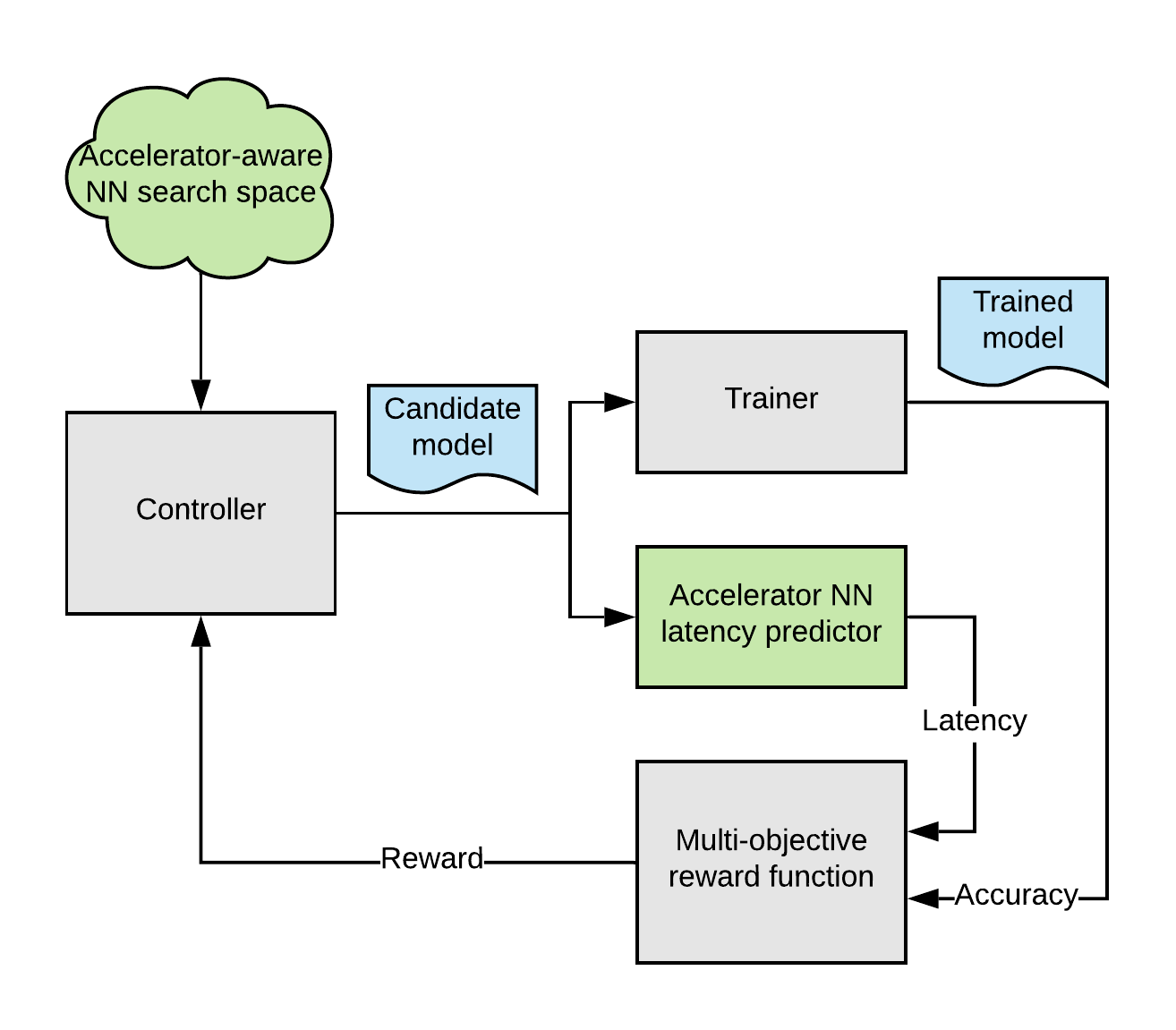
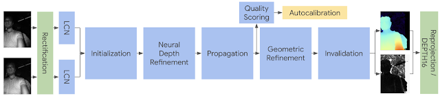
What Makes uDepth Distinct?
Stereo sensing systems can be extremely computationally intensive, and it’s critical that a sensor running at 30Hz is low power while remaining high quality. uDepth leverages a number of key insights to accomplish this.

One such insight is that given a pair of regions that are similar to each other, most corresponding subsets of those regions are also similar. For example, given two 8x8 patches of pixels that are similar, it is very likely that the top-left 4x4 sub-region of each member of the pair is also similar. This informs the uDepth pipeline’s initialization procedure, which builds a pyramid of depth proposals by comparison of non-overlapping tiles in each image and selecting those most similar. This process starts with 1x1 tiles, and accumulates support hierarchically until an initial low-resolution depth map is generated.

After initialization, we apply a novel technique for neural depth refinement to support the regular grid pattern illuminator on the Pixel 4. Typical active stereo systems project a pseudo-random grid pattern to help disambiguate matches in the scene, but uDepth is capable of supporting repeating grid patterns as well. Repeating structure in such patterns produces regions that look similar across stereo pairs, which can lead to incorrect matches. We mitigate this issue using a lightweight (75k parameter) convolutional architecture, using IR brightness and neighbor information to adjust incorrect matches — in less than 1.5ms per frame.
Neural depth refinement architecture.
Following neural depth refinement, good depth estimates are iteratively propagated from neighboring tiles. This and following pipeline steps leverage another insight key to the success of uDepth — natural scenes are typically locally planar with only small nonplanar deviations. This permits us to find planar tiles that cover the scene, and only later refine individual depths for each pixel in a tile, greatly reducing computational load.

Finally, the best match from among neighboring plane hypotheses is selected, with subpixel refinement and invalidation if no good match could be found.
Simplified depth architecture. Green components run on the GPU, yellow on the CPU, and blue on the Pixel Neural Core.
When a phone experiences a severe drop, it can result in the factory calibration of the stereo cameras diverging from the actual position of the cameras. To ensure high-quality results during real-world use, the uDepth system is self-calibrating. A scoring routine evaluates every depth image for signs of miscalibration, and builds up confidence in the state of the device. If miscalibration is detected, calibration parameters are regenerated from the current scene. This follows a pipeline consisting of feature detection and correspondence, subpixel refinement (taking advantage of the dot profile), and bundle adjustment.
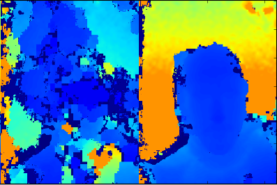
Left: Stereo depth with inaccurate calibration. Right: After autocalibration.
For more details, please refer to Slanted O(1) Stereo, upon which uDepth is based.

Depth for Computational Photography
The raw data from the uDepth sensor is designed to be accurate and metric, which is a fundamental requirement for Face Unlock. Computational photography applications such as portrait mode and 3D photos have very different needs. In these use cases, it is not critical to achieve video frame rates, but the depth should be smooth, edge-aligned and complete in the whole field-of-view of the color camera.
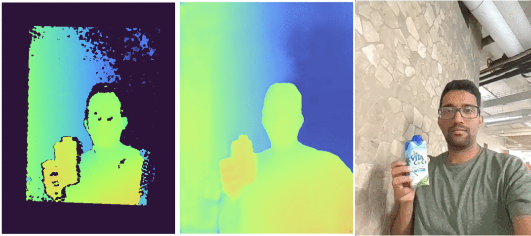
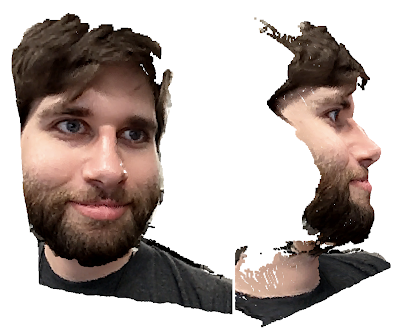
Left to right: raw depth sensing result, predicted depth, 3D photo. Notice the smooth rotation of the wall, demonstrating a continuous depth gradient rather than a single focal plane.
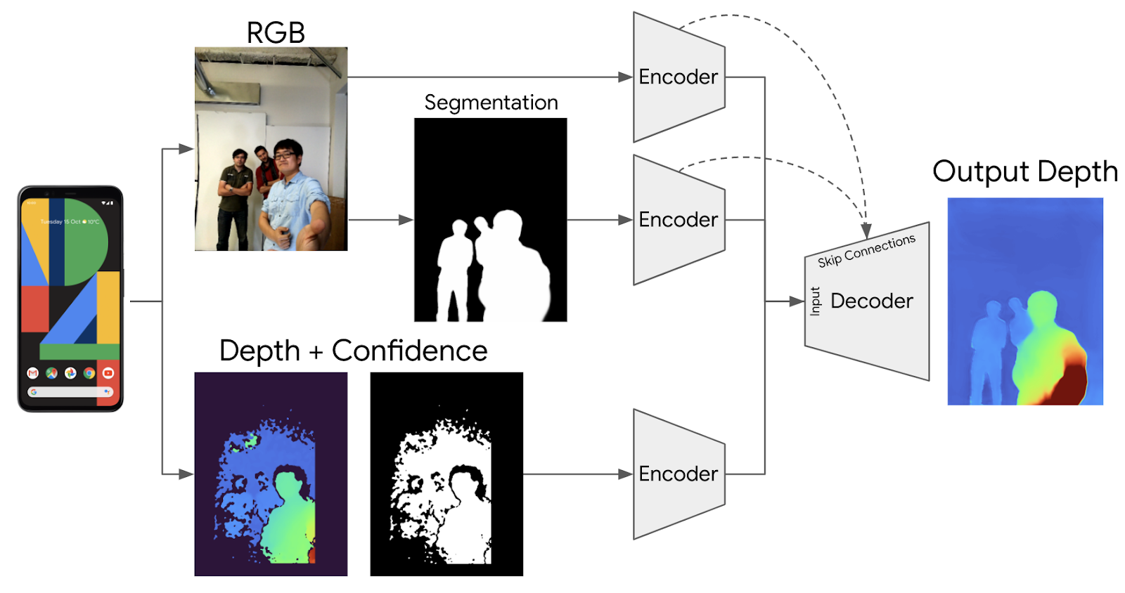
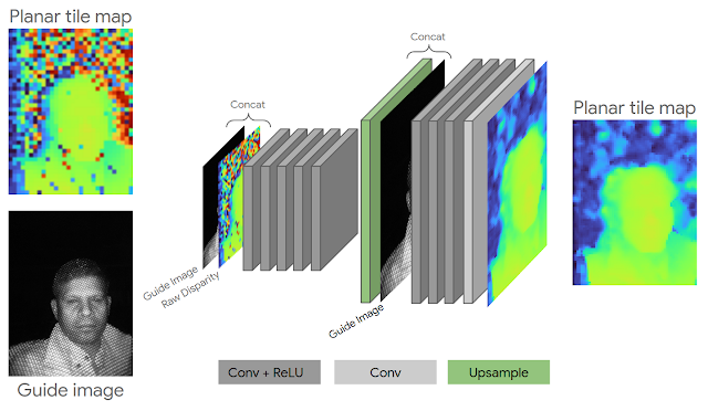
To achieve this we trained an end-to-end deep learning architecture that enhances the raw uDepth data, inferring a complete, dense 3D depth map. We use a combination of RGB images, people segmentation, and raw depth, with a dropout scheme forcing use of information for each of the inputs.
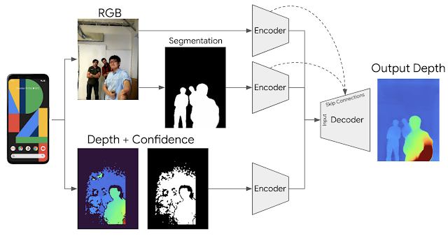
Architecture for computational photography depth enhancement.
To acquire ground truth, we leveraged a volumetric capture system that can produce near-photorealistic models of people using a geodesic sphere outfitted with 331 custom color LED lights, an array of high-resolution cameras, and a set of custom high-resolution depth sensors. We added Pixel 4 phones to the setup and synchronized them with the rest of the hardware (lights and cameras). The generated training data consists of a combination of real images as well as synthetic renderings from the Pixel 4 camera viewpoint.
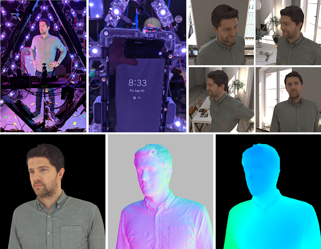
Data acquisition overview.
Putting It All Together
With all of these components in place, uDepth produces both a depth stream at 30Hz (exposed via Camera2), and smooth, post-processed depth maps for photography (exposed via Google Camera App when you take a depth-enabled selfie). The smooth, dense, per-pixel depth that our system produces is available on every Pixel 4 selfie with Social Media Depth features enabled, and can be used for post-capture effects such as bokeh and 3D photos for social media.
Example applications. Notice the multiple focal planes in the 3D photo on the right.
Finally, we are happy to provide a demo application for you to play with that visualizes a real-time point cloud from uDepth — download it here (this app is for demonstration and research purposes only and not intended for commercial use; Google will not provide any support or updates). This demo app visualizes 3D point clouds from your Pixel 4 device. Because the depth maps are time-synchronized and in the same coordinate system as the RGB images, a textured view of the 3D scene can be shown, as in the example visualization below:
Example single-frame, RGB point cloud from uDepth on the Pixel 4.
Acknowledgements
This work would not have been possible without the contributions of many, many people, including but not limited to Peter Barnum, Cheng Wang, Matthias Kramm, Jack Arendt, Scott Chung, Vaibhav Gupta, Clayton Kimber, Jeremy Swerdlow, Vladimir Tankovich, Christian Haene, Yinda Zhang, Sergio Orts Escolano, Sean Ryan Fanello, Anton Mikhailov, Philippe Bouchilloux, Mirko Schmidt, Ruofei Du, Karen Zhu, Charlie Wang, Jonathan Taylor, Katrina Passarella, Eric Meisner, Vitalii Dziuba, Ed Chang, Phil Davidson, Rohit Pandey, Pavel Podlipensky, David Kim, Jay Busch, Cynthia Socorro Herrera, Matt Whalen, Peter Lincoln, Geoff Harvey, Christoph Rhemann, Zhijie Deng, Daniel Finchelstein, Jing Pu, Chih-Chung Chang, Eddy Hsu, Tian-yi Lin, Sam Chang, Isaac Christensen, Donghui Han, Speth Chang, Zhijun He, Gabriel Nava, Jana Ehmann, Yichang Shih, Chia-Kai Liang, Isaac Reynolds, Dillon Sharlet, Steven Johnson, Zalman Stern, Jiawen Chen, Ricardo Martin Brualla, Supreeth Achar, Mike Mehlman, Brandon Barbello, Chris Breithaupt, Michael Rosenfield, Gopal Parupudi, Steve Goldberg, Tim Knight, Raj Singh, Shahram Izadi, as well as many other colleagues across Devices and Services, Google Research, Android and X. 

Source: Google AI Blog


EfficientNet-EdgeTPU: Creating Accelerator-Optimized Neural Networks with AutoML


For several decades, computer processors have doubled their performance every couple of years by reducing the size of the transistors inside each chip, as described by Moore’s Law. As reducing transistor size becomes more and more difficult, there is a renewed focus in the industry on developing domain-specific architectures — such as hardware accelerators — to continue advancing computational power. This is especially true for machine learning, where efforts are aimed at building specialized architectures for neural network (NN) acceleration. Ironically, while there has been a steady proliferation of these architectures in data centers and on edge computing platforms, the NNs that run on them are rarely customized to take advantage of the underlying hardware.

Today, we are happy to announce the release of EfficientNet-EdgeTPU, a family of image classification models derived from EfficientNets, but customized to run optimally on Google’s Edge TPU, a power-efficient hardware accelerator available to developers through the Coral Dev Board and a USB Accelerator. Through such model customizations, the Edge TPU is able to provide real-time image classification performance while simultaneously achieving accuracies typically seen only when running much larger, compute-heavy models in data centers.

Using AutoML to customize EfficientNets for Edge TPU
EfficientNets have been shown to achieve state-of-the-art accuracy in image classification tasks while significantly reducing the model size and computational complexity. To build EfficientNets designed to leverage the Edge TPU’s accelerator architecture, we invoked the AutoML MNAS framework and augmented the original EfficientNet’s neural network architecture search space with building blocks that execute efficiently on the Edge TPU (discussed below). We also built and integrated a “latency predictor” module that provides an estimate of the model latency when executing on the Edge TPU, by running the models on a cycle-accurate architectural simulator. The AutoML MNAS controller implements a reinforcement learning algorithm to search this space while attempting to maximize the reward, which is a joint function of the predicted latency and model accuracy. From past experience, we know that Edge TPU’s power efficiency and performance tend to be maximized when the model fits within its on-chip memory. Hence we also modified the reward function to generate a higher reward for models that satisfy this constraint.
Overall AutoML flow for designing customized EfficientNet-EdgeTPU models.
Search Space Design
When performing the architecture search described above, one must consider that EfficientNets rely primarily on depthwise-separable convolutions, a type of neural network block that factorizes a regular convolution to reduce the number of parameters as well as the amount of computations. However, for certain configurations, a regular convolution utilizes the Edge TPU architecture more efficiently and executes faster, despite the much larger amount of compute. While it is possible, albeit tedious, to manually craft a network that uses an optimal combination of the different building blocks, augmenting the AutoML search space with these accelerator-optimal blocks is a more scalable approach.
A regular 3x3 convolution (right) has more compute (multiply-and-accumulate (mac) operations) than an depthwise-separable convolution (left), but for certain input/output shapes, executes faster on Edge TPU due to ~3x more effective hardware utilization.
In addition, removing certain operations from the search space that require modifications to the Edge TPU compiler to fully support, such swish non-linearity and squeeze-and-excitation block, naturally leads to models that are readily ported to the Edge TPU hardware. These operations tend to improve model quality slightly, so by eliminating them from the search space, we have effectively instructed AutoML to discover alternate network architectures that may compensate for any potential loss in quality.

Model Performance
The neural architecture search (NAS) described above produced a baseline model, EfficientNet-EdgeTPU-S, which is subsequently scaled up using EfficientNet's compound scaling method to produce the -M and -L models. The compound scaling approach selects an optimal combination of input image resolution scaling, network width, and depth scaling to construct larger, more accurate models. The -M, and -L models achieve higher accuracy at the cost of increased latency as shown in the figure below.
EfficientNet-EdgeTPU-S/M/L models achieve better latency and accuracy than existing EfficientNets (B1), ResNet, and Inception by specializing the network architecture for Edge TPU hardware. In particular, our EfficientNet-EdgeTPU-S achieves higher accuracy, yet runs 10x faster than ResNet-50.
Interestingly, the NAS-generated model employs the regular convolution quite extensively in the initial part of the network where the depthwise-separable convolution tends to be less effective than the regular convolution when executed on the accelerator. This clearly highlights the fact that trade-offs usually made while optimizing models for general purpose CPUs (reducing the total number of operations, for example) are not necessarily optimal for hardware accelerators. Also, these models achieve high accuracy even without the use of esoteric operations. Comparing with the other image classification models such as Inception-resnet-v2 and Resnet50, EfficientNet-EdgeTPU models are not only more accurate, but also run faster on Edge TPUs.

This work represents a first experiment in building accelerator-optimized models using AutoML. The AutoML-based model customization can be extended to not only a wide range of hardware accelerators, but also to several different applications that rely on neural networks.

From Cloud TPU training to Edge TPU deployment
We have released the training code and pretrained models for EfficientNet-EdgeTPU on our github repository. We employ tensorflow’s post-training quantization tool to convert a floating-point trained model to an Edge TPU-compatible integer-quantized model. For these models, the post-training quantization works remarkably well and produces only a very slight loss in accuracy (~0.5%). The script for exporting the quantized model from a training checkpoint can be found here. For an update on the Coral platform, see this post on the Google Developer’s Blog, and for full reference materials and detailed instructions, please refer to the Coral website.

Acknowledgements
Special thanks to Quoc Le, Hongkun Yu, Yunlu Li, Ruoming Pang, and Vijay Vasudevan from the Google Brain team; Bo Wu, Vikram Tank, and Ajay Nair from the Google Coral team; Han Vanholder, Ravi Narayanaswami, John Joseph, Dong Hyuk Woo, Raksit Ashok, Jason Jong Kyu Park, Jack Liu, Mohammadali Ghodrat, Cao Gao, Berkin Akin, Liang-Yun Wang, Chirag Gandhi, and Dongdong Li from the Google Edge TPU team.

Source: Google AI Blog


Glass Enterprise Edition 2: faster and more helpful

Glass Enterprise Edition has helped workers in a variety of industries—from logistics, to  manufacturing, to field services—do their jobs more efficiently by providing hands-free access to the information and tools they need to complete their work. Workers can use Glass to access checklists, view instructions or send inspection photos or videos, and our enterprise customers have reported faster production times, improved quality, and reduced costs after using Glass.


Glass Enterprise Edition 2 helps businesses further improve the efficiency of their employees. As our customers have adopted Glass, we’ve received valuable feedback that directly informed the improvements in Glass Enterprise Edition 2. 

Glass Enterprise Edition 2.png
Glass Enterprise Edition 2 with safety frames by Smith Optics. Glass is a small, lightweight

wearable computer with a transparent display for hands-free work.

Glass Enterprise Edition 2 is built on the Qualcomm Snapdragon XR1 platform, which features a significantly more powerful multicore CPU (central processing unit) and a new artificial intelligence engine. This enables significant power savings, enhanced performance and support for computer vision and advanced machine learning capabilities. We’ve also partnered with Smith Optics to make Glass-compatible safety frames for different types of demanding work environments, like manufacturing floors and maintenance facilities.

Additionally, Glass Enterprise Edition 2 features improved camera performance and quality, which builds on Glass’s existing first person video streaming and collaboration features. We’ve also added USB-C port that supports faster charging, and increased overall battery life to enable customers to use Glass longer between charges.

Finally, Glass Enterprise Edition 2 is easier to develop for and deploy. It’s built on Android, making it easier for customers to integrate the services and APIs (application programming interfaces) they already use. And in order to support scaled deployments, Glass Enterprise Edition 2 now supports Android Enterprise Mobile Device Management.

Over the past two years atX, Alphabet’s moonshot factory, we’ve collaborated with our partners to provide solutions that improve workplace productivity for a growing number of customers—including AGCO, Deutsche Post DHL Group, Sutter Health, and H.B. Fuller. We’ve been inspired by the ways businesses like these have been using Glass Enterprise Edition. X, which is designed to be a protected space for long-term thinking and experimentation, has been a great environment in which to learn and refine the Glass product. Now, in order to meet the demands of the growing market for wearables in the workplace and to better scale our enterprise efforts, the Glass team has moved from X to Google.

We’re committed to providing enterprises with the helpful tools they need to work better, smarter and faster. Enterprise businesses interested in using Glass Enterprise Edition 2 can contact our sales team or our network of Glass Enterprise solution partners starting today. We’re excited to see how our partners and customers will continue to use Glass to shape the future of work.

On the Path to Cryogenic Control of Quantum Processors


Building a quantum computer that can solve practical problems that would otherwise be classically intractable due to the computation complexity, cost, energy consumption or time to solution, is the longstanding goal of the Google AI Quantum team. Current thresholds suggest a first generation error-corrected quantum computer will require on the order of 1 million physical qubits, which is more than four orders of magnitude more qubits than exist in Bristlecone, our 72 qubit quantum processor. Increasing the number of physical qubits needed for a fault-tolerant quantum computer while maintaining high-quality control of each qubit are intertwined and exciting technological challenges that will require inventions beyond simply copying and pasting our current control architecture. One critical challenge is reducing the number of input/output control lines per qubit by relocating the room temperature analog control electronics to the 3 kelvin stage in the cryostat, while maintaining high-quality qubit control.

As a step towards solving that challenge, this week we presented our first generation cryogenic-CMOS single-qubit controller at the International Solid State Circuits Conference in San Francisco. Fabricated using commercial CMOS technology, our controller operates at 3 kelvin, consumes less than 2 milliwatts of power and measures just 1 mm by 1.6 mm. Functionally, it provides an instruction set for single-qubit gate operations, providing analog control of a qubit via digital lines between room temperature and 3 kelvin, all while consuming ~1000 times less power compared to our current room temperature control electronics.
Google’s first generation cryogenic-CMOS single-qubit controller (center and zoomed on the right) packaged and ready to be deployed inside our cryostat. The controller measures 1mm by 1.6mm.
How to Control 72 Qubits
In our lab in Santa Barbara, we run programs on Bristlecone by applying gigahertz frequency analog control signals to each of the qubits to manipulate the qubit state, to entangle qubits and to measure the outcomes of our computations. How well we define the shape and frequency of these control signals directly impacts the quality of our computation. To make high-quality qubit control signals, we leverage technology developed for smartphones packaged in server racks at room temperature. Individual coaxial cables deliver these signals to each qubit, which are themselves kept inside a cryostat chilled to 10 millikelvin. While this approach makes sense for a Bristlecone-scale quantum processor, which demands 2 control lines per qubit for 144 unique control signals, we realized that a more integrated approach would be required in order to scale our systems to the million qubit level.
Research Scientist Amit Vainsencher checking the wiring on Bristlecone in one of Google's flagship cryostats. Blue coaxial cables are connected from custom analog control electronics (server rack on the right) to the quantum processor.
In our current setup, the number of physical wires connected from room temperature to the qubits inside the cryostat and the finite cooling power of the cryostat represent a significant constraint. One way to alleviate this is to move the digital to analog control closer to the quantum processor. Currently, our room temperature digital-to-analog waveform generators used to control individual qubits, dissipate ~1 watt of waste heat per qubit. The cooling power of our cryostat at 3 kelvin is 0.1 watt. That means if we crammed 150 waveform generators into our cryostat (never mind the limited physical space inside the refrigerator for a moment) we would overwhelm the cooling power of our cryostat by 1500x, thereby cooking our cryostat and rendering our qubits useless. Therefore, simply installing our existing digital-to-analog control in the cryostat will not set us on the path to control millions of qubits. It is clear we need an integrated low-power qubit control solution.

A Cool Idea
In collaboration with University of Massachusetts Professor Joseph Bardin, we set out to develop custom integrated circuits (ICs) to control our qubits from within the cryostat to ultimately reduce the physical I/O connections to and from our future quantum processors. These ICs would be designed to operate in the ultracold environment, specifically 3 kelvin, and turn digital instructions into analog control pulses for qubits. A key research objective was to first design a custom IC with low power requirements, in order to prevent warming up the cryostat.

We designed our IC to dissipate no more than 2 milliwatts of power at 3 kelvin, which can be challenging as most physical CMOS models assume operation closer to 300 kelvin. After design and fabrication of the IC with the low power design constraints in mind, we verified that the cryogenic-CMOS qubit controller worked at room temperature. We then mounted it in our cryostat at 3 kelvin and connected it to a qubit (mounted at 10 millikelvin in the same cryostat). We carried out a series of experiments to establish that the cryogenic-CMOS qubit controller worked as designed, and most importantly, that we hadn't just installed a heater inside our cryostat.
Schematic of the cryogenic-CMOS qubit controller mounted on the 3 kelvin stage of our dilution refrigerator and connected to a qubit. Our standard qubit control electronics were connected in parallel to enable control and measurement of the qubit as an in-situ check experiment.
Performance at Low Temperature
Baseline experiments for our new quantum control hardware, including T1, Rabi oscillations, and single qubit gates, show similar performance compared to our standard room-temperature qubit control electronics: qubit coherence time was virtually unchanged, and high-visibility Rabi oscillations were observed by varying the amplitude of the pulses out of the cryogenic-CMOS qubit controller—a signature response of a driven qubit.

Comparison of the qubit coherence time measured using the standard and cryogenic quantum controllers.
Measured Rabi amplitude oscillations using the cryogenic controller. The green and black traces are the probability of measuring the qubits in the 1 and 0 states, respectively.
Next Steps
Although all of these results are promising, this first generation cryogenic-CMOS qubit controller is but one small step towards a truly scalable qubit control and measurement system. For instance, our controller is only able to address a single qubit, and it still requires several connections to room temperature. In addition, we still need to work hard to quantify the error rates for single qubit gates. As such, we are excited to reduce the energy required to control qubits and still maintain the delicate control required to perform high-quality qubit operations.

Acknowledgements
This work was carried out with the support of the Google Visiting Researcher Program while Prof. Bardin, an Associate Professor with the University of Massachusetts Amherst, was on sabbatical with the Google AI Quantum Team. This work would not have been possible without the many contributions of members of the Google AI Quantum team, especially Evan Jeffrey for his integration of the cryo-CMOS controller into the qubit calibration software, Ted White for his on-demand qubit calibrations and Trent Huang for his tireless design rules checks.

Source: Google AI Blog


5 reasons to love the new Chromecast

https://lh4.googleusercontent.com/uJ_Dwg_g96eXtKUqTx2d4oDIlfRzJ0gWzG1LhgMXEwC-02oRIvsaTMM3svbAvudvGkVoBf53g3rqVvyDPvti4oJ6jaBox7aNBzS2jM6nww0j6o9xQar1NYFuSyJwU_z3IQEonJAH


We launched our first Chromecast in 2013 with the aim to make it easy to get your favorite content right from your phone to your TV. With hundreds of compatible apps to cast from, people are tapping the Cast button more than ever. And since Chromecast, the Made by Google family of products has continued to grow, bringing the best of hardware, software, and AI together. So for this 5th year of Chromecast, we wanted to share the top 5 reasons we’re excited about our newest Chromecast:
  1. Fits right in. With a new design, Chromecast blends in with your decor and the rest of the Made by Google family.
  2. Stream hands-free. Chromecast and Google Home work seamlessly together. Just say what you want to watch from compatible services, like YouTube or Netflix, and control your TV just by asking. Try, “Hey Google, play Lost in Space from Netflix.” (You’ll need a Netflix subscription to get started.)
  3. Picture perfect at 60fps. Our newest Chromecast supports streaming in 1080p at 60 frames per second, giving you a more lifelike image. So when you’re watching the match, it will feel even more like you’re there.
  4. More than a screen, it’s a canvas. With Ambient Mode, you can personalize your TV with a constantly updating stream of the best and latest photos taken by you, your friends and your family from Google Photos. With new Live Albums from Google Photos, you can enjoy photos of people and pets you care about and skip blurry photos and duplicates -- all without lifting a finger. New photos will show up automatically on your TV -- no uploading hassles.
  5. And it has an MRP of just ₹3,499. So it’s the perfect gift this upcoming holiday season for the streamer in your life.
    The new Chromecast is available in Charcoal starting today exclusively from Flipkart, and comes with a one-year Sony LIV Premium subscription along with a six-month Gaana Plus subscription.
    So go ahead, #StreamOn!
    Posted by Jess Bonner,  Chromecast PM