Tag Archives: hardware

Open source PDKs joining the Linux Foundation’s CHIPS Alliance

In November 2020, we launched our Open Source MPW Shuttle Program to make it easier for researchers and developers to build custom silicon and to enable a thriving ecosystem around open source hardware. Working with our partner, SkyWater Technology, we released the first foundry-supported open source process design kit (PDK) for their 130nm mixed-signal CMOS technology (SKY130), then welcomed GlobalFoundries as a partner with the release of an open source PDK for their 180nm MCU process (GF180MCU).

Then, to give researchers and developers a way to validate and prove their designs made with the PDKs, we partnered with Efabless to fund a series of no-cost manufacturing shuttles for open source designs. In support of this program, Efabless released an end-to-end RTL to GDS design stack called OpenLane that is open source, freely available, and fully supported by their manufacturing platform. OpenLane is now being maintained as part of the OpenROAD Project. When combined with open source PDKs, a design’s verification results can now be freely shared and easily replicated by other researchers and developers, which has enabled a new collaborative model to evaluate and iterate on ideas.

Pictures of a full wafer from the first SKY130 shuttle, a tray of bare dies, and a project bring-up from SKY130 MPW-2.

Results

The Open Source MPW Shuttle Program has been a success and we’re excited by the growth we’ve seen in this ecosystem. Since its inception, the program has launched eight shuttle runs on SKY130 and an initial test run on GF180MCU, the last of which are being packaged now. With 40 slots per shuttle, we’ve manufactured 360 designs out of over 600 submissions from 19 countries around the world.Graph showing number of designs submitted to Open Source MPW shuttles across versions 1 through 8

The program has also fostered collaboration between the open source community and Google. We’ve learned valuable lessons from designers who participated in the program giving feedback and filing hundreds of bugs and pull requests. These have helped to improve each successive run and to make the platforms and tools more feature-complete.

Elsewhere in the ecosystem, we’re excited by the release of new open source PDKs from foundries like the 130nm BiCMOS process from IHP, the SOI-CMOS PDK from Minimal Fab, and also by the publication of new semiconductor research using open source PDKs. Multiple universities have incorporated open source PDKs into their curriculum, and last year, NIST adopted the SKY130 PDK to migrate their existing planarized wafer designs for nanotechnology research.

Announcing GF180MCU MPW-1

We’ve just launched a new MPW-1 shuttle for GF180MCU in our partnership with Efabless. Submissions will be accepted until December 11th, targeting delivery in early 2024.

Graph showing number of designs submitted to Open Source MPW shuttles across versions 1 through 8

Next Steps

The open source silicon ecosystem is continuing to grow and evolve. After GF180 MPW-1 concludes, the open source SKY130 and GF180MCU PDKs will be joining the Linux Foundation’s CHIPS Alliance under a new working group to foster continued open source PDK development, and we expect future PDK releases will join as well. This will help with the transition to a broader governance model that enables more participation by industry, academia and the community, opening the possibility for larger shuttle programs with multiple sponsors as the ecosystem continues to grow.

Low-cost manufacturing options will continue to be available through this transition, both through commercial shuttle offerings like Efabless’ ChipIgnite program and also through educational efforts like TinyTapeout.

Thank you

Lastly, we’d like to thank the open source community. Your feedback has been invaluable to the success so far, and has helped to improve the tools and documentation to be more user-friendly. We have also seen contributions from the community in the form of hundreds of new and fully manufacturable designs, which have helped to expand the range and capabilities of open source hardware available to the community. We look forward to continuing partnerships to build a thriving ecosystem around open source silicon.

By Aaron Cunningham – Technical Program Manager, Core Hardware Tools

Barkour: Benchmarking animal-level agility with quadruped robots

Creating robots that exhibit robust and dynamic locomotion capabilities, similar to animals or humans, has been a long-standing goal in the robotics community. In addition to completing tasks quickly and efficiently, agility allows legged robots to move through complex environments that are otherwise difficult to traverse. Researchers at Google have been pursuing agility for multiple years and across various form factors. Yet, while researchers have enabled robots to hike or jump over some obstacles, there is still no generally accepted benchmark that comprehensively measures robot agility or mobility. In contrast, benchmarks are driving forces behind the development of machine learning, such as ImageNet for computer vision, and OpenAI Gym for reinforcement learning (RL).

In “Barkour: Benchmarking Animal-level Agility with Quadruped Robots”, we introduce the Barkour agility benchmark for quadruped robots, along with a Transformer-based generalist locomotion policy. Inspired by dog agility competitions, a legged robot must sequentially display a variety of skills, including moving in different directions, traversing uneven terrains, and jumping over obstacles within a limited timeframe to successfully complete the benchmark. By providing a diverse and challenging obstacle course, the Barkour benchmark encourages researchers to develop locomotion controllers that move fast in a controllable and versatile way. Furthermore, by tying the performance metric to real dog performance, we provide an intuitive metric to understand the robot performance with respect to their animal counterparts.


We invited a handful of dooglers to try the obstacle course to ensure that our agility objectives were realistic and challenging. Small dogs complete the obstacle course in approximately 10s, whereas our robot’s typical performance hovers around 20s.


Barkour benchmark

The Barkour scoring system uses a per obstacle and an overall course target time based on the target speed of small dogs in the novice agility competitions (about 1.7m/s). Barkour scores range from 0 to 1, with 1 corresponding to the robot successfully traversing all the obstacles along the course within the allotted time of approximately 10 seconds, the average time needed for a similar-sized dog to traverse the course. The robot receives penalties for skipping, failing obstacles, or moving too slowly.

Our standard course consists of four unique obstacles in a 5m x 5m area. This is a denser and smaller setup than a typical dog competition to allow for easy deployment in a robotics lab. Beginning at the start table, the robot needs to weave through a set of poles, climb an A-frame, clear a 0.5m broad jump and then step onto the end table. We chose this subset of obstacles because they test a diverse set of skills while keeping the setup within a small footprint. As is the case for real dog agility competitions, the Barkour benchmark can be easily adapted to a larger course area and may incorporate a variable number of obstacles and course configurations.

Overview of the Barkour benchmark’s obstacle course setup, which consists of weave poles, an A-frame, a broad jump, and pause tables. The intuitive scoring mechanism, inspired by dog agility competitions, balances speed, agility and performance and can be easily modified to incorporate other types of obstacles or course configurations.


Learning agile locomotion skills

The Barkour benchmark features a diverse set of obstacles and a delayed reward system, which pose a significant challenge when training a single policy that can complete the entire obstacle course. So in order to set a strong performance baseline and demonstrate the effectiveness of the benchmark for robotic agility research, we adopt a student-teacher framework combined with a zero-shot sim-to-real approach. First, we train individual specialist locomotion skills (teacher) for different obstacles using on-policy RL methods. In particular, we leverage recent advances in large-scale parallel simulation to equip the robot with individual skills, including walking, slope climbing, and jumping policies.

Next, we train a single policy (student) that performs all the skills and transitions in between by using a student-teacher framework, based on the specialist skills we previously trained. We use simulation rollouts to create datasets of state-action pairs for each one of the specialist skills. This dataset is then distilled into a single Transformer-based generalist locomotion policy, which can handle various terrains and adjust the robot's gait based on the perceived environment and the robot’s state.

During deployment, we pair the locomotion transformer policy that is capable of performing multiple skills with a navigation controller that provides velocity commands based on the robot's position. Our trained policy controls the robot based on the robot's surroundings represented as an elevation map, velocity commands, and on-board sensory information provided by the robot.


Deployment pipeline for the locomotion transformer architecture. At deployment time, a high-level navigation controller guides the real robot through the obstacle course by sending commands to the locomotion transformer policy.

Robustness and repeatability are difficult to achieve when we aim for peak performance and maximum speed. Sometimes, the robot might fail when overcoming an obstacle in an agile way. To handle failures we train a recovery policy that quickly gets the robot back on its feet, allowing it to continue the episode.


Evaluation

We evaluate the Transformer-based generalist locomotion policy using custom-built quadruped robots and show that by optimizing for the proposed benchmark, we obtain agile, robust, and versatile skills for our robot in the real world. We further provide analysis for various design choices in our system and their impact on the system performance.

Model of the custom-built robots used for evaluation.

We deploy both the specialist and generalist policies to hardware (zero-shot sim-to-real). The robot’s target trajectory is provided by a set of waypoints along the various obstacles. In the case of the specialist policies, we switch between specialist policies by using a hand-tuned policy switching mechanism that selects the most suitable policy given the robot’s position.


Typical performance of our agile locomotion policies on the Barkour benchmark. Our custom-built quadruped robot robustly navigates the terrain’s obstacles by leveraging various skills learned using RL in simulation.

We find that very often our policies can handle unexpected events or even hardware degradation resulting in good average performance, but failures are still possible. As illustrated in the image below, in case of failures, our recovery policy quickly gets the robot back on its feet, allowing it to continue the episode. By combining the recovery policy with a simple walk-back-to-start policy, we are able to run repeated experiments with minimal human intervention to measure the robustness.


Qualitative example of robustness and recovery behaviors. The robot trips and rolls over after heading down the A-frame. This triggers the recovery policy, which enables the robot to get back up and continue the course.

We find that across a large number of evaluations, the single generalist locomotion transformer policy and the specialist policies with the policy switching mechanism achieve similar performance. The locomotion transformer policy has a slightly lower average Barkour score, but exhibits smoother transitions between behaviors and gaits.


Measuring robustness of the different policies across a large number of runs on the Barkour benchmark.

Histogram of the agility scores for the locomotion transformer policy. The highest scores shown in blue (0.75 - 0.9) represent the runs where the robot successfully completes all obstacles.


Conclusion

We believe that developing a benchmark for legged robotics is an important first step in quantifying progress toward animal-level agility. To establish a strong baseline, we investigated a zero-shot sim-to-real approach, taking advantage of large-scale parallel simulation and recent advancements in training Transformer-based architectures. Our findings demonstrate that Barkour is a challenging benchmark that can be easily customized, and that our learning-based method for solving the benchmark provides a quadruped robot with a single low-level policy that can perform a variety of agile low-level skills.


Acknowledgments

The authors of this post are now part of Google DeepMind. We would like to thank our co-authors at Google DeepMind and our collaborators at Google Research: Wenhao Yu, J. Chase Kew, Tingnan Zhang, Daniel Freeman, Kuang-Hei Lee, Lisa Lee, Stefano Saliceti, Vincent Zhuang, Nathan Batchelor, Steven Bohez, Federico Casarini, Jose Enrique Chen, Omar Cortes, Erwin Coumans, Adil Dostmohamed, Gabriel Dulac-Arnold, Alejandro Escontrela, Erik Frey, Roland Hafner, Deepali Jain, Yuheng Kuang, Edward Lee, Linda Luu, Ofir Nachum, Ken Oslund, Jason Powell, Diego Reyes, Francesco Romano, Feresteh Sadeghi, Ron Sloat, Baruch Tabanpour, Daniel Zheng, Michael Neunert, Raia Hadsell, Nicolas Heess, Francesco Nori, Jeff Seto, Carolina Parada, Vikas Sindhwani, Vincent Vanhoucke, and Jie Tan. We would also like to thank Marissa Giustina, Ben Jyenis, Gus Kouretas, Nubby Lee, James Lubin, Sherry Moore, Thinh Nguyen, Krista Reymann, Satoshi Kataoka, Trish Blazina, and the members of the robotics team at Google DeepMind for their contributions to the project.

Source: Google AI Blog


PJRT: Simplifying ML Hardware and Framework Integration

Infrastructure fragmentation in Machine Learning (ML) across frameworks, compilers, and runtimes makes developing new hardware and toolchains challenging. This inhibits the industry’s ability to quickly productionize ML-driven advancements. To simplify the growing complexity of ML workload execution across hardware and frameworks, we are excited to introduce PJRT and open source it as part of the recently available OpenXLA Project.

PJRT (used in conjunction with OpenXLA’s StableHLO) provides a hardware- and framework-independent interface for compilers and runtimes. It simplifies the integration of hardware with frameworks, accelerating framework coverage for the hardware, and thus hardware targetability for workload execution.

PJRT is the primary interface for TensorFlow and JAX and fully supported for PyTorch, and is well integrated with the OpenXLA ecosystem to execute workloads on TPU, GPU, and CPU. It is also the default runtime execution path for most of Google’s internal production workloads. The toolchain-independent architecture of PJRT allows it to be leveraged by any hardware, framework, or compiler, with extensibility for unique features. With this open-source release, we're excited to allow anyone to begin leveraging PJRT for their own devices.

If you’re developing an ML hardware accelerator or developing your own compiler and runtime, check out the PJRT source code on GitHub and sign up for the OpenXLA mailing list to quickly bootstrap your work.

Vision: Simplifying ML Hardware and Framework Integration

We are entering a world of ambient experiences where intelligent apps and devices surround us, from edge to the cloud, in a range of environments and scales. ML workload execution currently supports a combinatorial matrix of hardware, frameworks, and workflows, mostly through tight vertical integrations. Examples of such vertical integrations include specific kernels for TPU versus GPU, specific toolchains to train and serve in TensorFlow versus PyTorch. These bespoke 1:1 integrations are perfectly valid solutions but promote lock-in, inhibit innovation, and are expensive to maintain. This problem of a fragmented software stack is compounded over time as different computing hardware needs to be supported.

A variety of ML hardware exists today and hardware diversity is expected to increase in the future. ML users have options and they want to exercise them seamlessly: users want to train a large language model (LLM) on TPU in the Cloud, batch infer on GPU or even CPU, distill, quantize, and finally serve them on mobile processors. Our goal is to solve the challenge of making ML workloads portable across hardware by making it easy to integrate the hardware into the ML infrastructure (framework, compiler, runtime).

Portability: Seamless Execution

The workflow to enable this vision with PJRT is as follows (shown in Figure 1):

  1. The hardware-specific compiler and runtime provider implement the PJRT API, package it as a plugin containing the compiler and runtime hooks, and register it with the frameworks. The implementation can be opaque to the frameworks.
  2. The frameworks discover and load one or multiple PJRT plugins as dynamic libraries targeting the hardware on which to execute the workload.
  3. That’s it! Execute the workload from the framework onto the target hardware.

The PJRT API will be backward compatible. The plugin would not need to change often and would be able to do version-checking for features.

Diagram of PJRT architecture
Figure 1: To target specific hardware, provide an implementation of the PJRT API to package a compiler and runtime plugin that can be called by the framework.

Cohesive Ecosystem

As a foundational pillar of the OpenXLA Project, PJRT is well-integrated with projects within the OpenXLA Project including StableHLO and the OpenXLA compilers (XLA, IREE). It is the primary interface for TensorFlow and JAX and fully supported for PyTorch through PyTorch/XLA. It provides the hardware interface layer in solving the combinatorial framework x hardware ML infrastructure fragmentation (see Figure 2).

Diagram of PJRT hardware interface layer
Figure 2: PJRT provides the hardware interface layer in solving the combinatorial framework x hardware ML infrastructure fragmentation, well-integrated with OpenXLA.

Toolchain Independent

PJRT is hardware and framework independent. With framework integration through the self-contained IR StableHLO, PJRT is not coupled with a specific compiler, and can be used outside of the OpenXLA ecosystem, including with other proprietary compilers. The public availability and toolchain-independent architecture allows it to be used by any hardware, framework or compiler, with extensibility for unique features. If you are developing an ML hardware accelerator, compiler, or runtime targeting any hardware, or converging siloed toolchains to solve infrastructure fragmentation, PJRT can minimize bespoke hardware and framework integration, providing greater coverage and improving time-to-market at lower development cost.

Driving Impact with Collaboration

Industry partners such as Intel and others have already adopted PJRT.

Intel

Intel is leveraging PJRT in Intel® Extension for TensorFlow to provide the Intel GPU backend for TensorFlow and JAX. This implementation is based on the PJRT plugin mechanism (see RFC). Check out how this greatly simplifies the framework and hardware integration with this example of executing a JAX program on Intel GPU.

"At Intel, we share Google's vision of modular interfaces to make integration easier and enable faster, framework-independent development. Similar in design to the PluggableDevice mechanism, PJRT is a pluggable interface that allows us to easily compile and execute XLA's High Level Operations on Intel devices. Its simple design allowed us to quickly integrate it into our systems and start running JAX workloads on Intel® GPUs within just a few months. PJRT enables us to more efficiently deliver hardware acceleration and oneAPI-powered AI software optimizations to developers using a wide range of AI Frameworks." - Wei Li, VP and GM, Artificial Intelligence and Analytics, Intel.

Technology Leader

We’re also working with a technology leader to leverage PJRT to provide the backend targeting their proprietary processor for JAX. More details on this to follow soon.

Get Involved

PJRT is available on GitHub: source code for the API and a reference openxla-pjrt-plugin, and integration guides. If you develop ML frameworks, compilers, or runtimes, or are interested in improving portability of workloads across hardware, we want your feedback. We encourage you to contribute code, design ideas, and feature suggestions. We also invite you to join the OpenXLA mailing list to stay updated with the latest product and community announcements and to help shape the future of an interoperable ML infrastructure.

Acknowledgements

Allen Hutchison, Andrew Leaver, Chuanhao Zhuge, Jack Cao, Jacques Pienaar, Jieying Luo, Penporn Koanantakool, Peter Hawkins, Robert Hundt, Russell Power, Sagarika Chalasani, Skye Wanderman-Milne, Stella Laurenzo, Will Cromar, Xiao Yu.

By Aman Verma, Product Manager, Machine Learning Infrastructure

Google and NIST partner on nanotechnology development platform

We’re proud to announce Google’s cooperative research and development agreement with the U.S. National Institute of Standards and Technology (NIST) to develop an open source testbed for nanotechnology research and development for American universities. NIST—a bureau of the U.S. Department of Commerce—will start by migrating their existing planarized wafer designs to an open source framework, which can be manufactured in the U.S. on SkyWater Technologies’ open source 130nm process (SKY130). The physical wafers and source code will be available in the coming months. Together, NIST, Google, and the open source community will develop designs to facilitate research into both basic and applied science, including technology transfer into production with U.S. manufacturers.

Furthering Google’s goals to improve access to semiconductor technology, this agreement will provide academic researchers with unprecedented resources from a semiconductor foundry to enhance research into the physics of semiconductors and nanodevices. This includes their chemistry, defects, electrical properties, high frequency operation, and switching behavior, while reducing overall costs through economies of scale. Most importantly, this access enhances the technology transfer process by enabling researchers to develop new and emerging technologies using foundry resources, that can then be seamlessly transitioned into mass production since universities will already be using an industrially relevant platform. This will greatly improve scientist’s ability to move their technologies through the tech-transfer “valley of death” and into practical use.

Nanotechnology research has benefitted from silicon wafers that are normally used for chip manufacturing in a unique way. Instead of turning them into packaged microchips, their smooth, planarized surface makes a great substrate for building and testing nanoscale structures. This likewise helps test their transition into mass production.

Picture of a full wafer using the SKY130 open source PDK.

Picture of a full wafer using the SKY130 open source PDK.


The wafer for this platform has a number of different metrology structures, from parametric test structures based on simple transistor arrays—which can be probed in a probe station—to thousands of complex measurements that users can operate using synthesized digital circuits. Critically, the wafers will be available to universities in a 200 mm form factor, and mid-production planarized wafers with less than a single nanometer of surface roughness. Smooth, flat surfaces are critical for advanced manufacturing at small sizes.

NIST researchers are also ensuring that the wafers have photolithographic and electron beam alignment marks commonly found in university nanofabrication facilities, allowing the foundry silicon to be used directly by university researchers with ease. Metal pads on the surface will allow scientists to access the semiconductor transistors from the surface.

NIST scientists anticipate the nanotechnology accelerator platform will enhance scientific investigations into a diverse set of technologies, including memory devices (resistive switches, magnetic tunnel junctions, flash memories), artificial intelligence, plasmonics, semiconductor bioelectronics, thin film transistors and even quantum information science.

Picture of a development die from Google 's OpenMPW program for the nanotechnology accelerator developed by NIST and the University of Michigan

Picture of a development die from Google 's OpenMPW program for the nanotechnology accelerator developed by NIST and the University of Michigan

This program also benefits from Google’s previous contributions and support of the GDSFactory and OpenFASOC open source projects that help automate and shorten the construction of these important measuring devices from months to days. Ahead of the full wafer tapeout in 2023, NIST scientists, working with partners at the University of Michigan, Carnegie Mellon, University of Maryland, The George Washington University, and Brown University have been using Google's OpenMPW program to develop and test preliminary circuits which they expect to include in the nanotechnology accelerator. Preliminary testing will help ensure the program’s goals are met with working circuits that best serve the scientific community.

A key factor in cutting-edge research is reproducibility, or the ability for researchers from different institutions to repeat each other’s experiments and improve upon them. By migrating to an open source framework, researchers can more easily share reproducible results, contribute to the creation of open source datasets to enhance future simulation, and advance the scientific community’s state of the art of nanotechnology and semiconductor manufacturing.

NIST and Google will distribute the first production run of wafers to leading U.S. universities. Post-program, American scientists will be able to directly purchase the wafers from Skywater without license requirements, giving them the freedom to pursue their research without any restrictions. Since wafers are hundreds of times cheaper than full mask-sets or the cost of designing integrated circuits from scratch, scientists will have a much easier time getting and using this powerful industrial technology. Longer term, working with NIST to develop future platforms on the recently announced SKY90FD open source PDK will further expand this R&D ecosystem.

To kick off this research effort NIST is organizing the "NIST Integrated Circuits for Metrology Workshop" from September 20–21, 2022. This workshop will be held online with a series of presentations and panel discussions on the first day. During the second day, a working group of researchers, scientists and engineers will work to focus on the creation of parametric test structures for monolithic integration using open source silicon technology. Visit the event website to get more details about this program and register to attend or learn more about presenting.

By Ethan Mahintorabi and Johan Euphrosine, Software Engineers – Hardware Toolchains Team, and Aaron Cunningham, Technical Program Manager – Google Open Source Programs Office

Hidden Interfaces for Ambient Computing

As consumer electronics and internet-connected appliances are becoming more common, homes are beginning to embrace various types of connected devices that offer functionality like music control, voice assistance, and home automation. A graceful integration of devices requires adaptation to existing aesthetics and user styles rather than simply adding screens, which can easily disrupt a visual space, especially when they become monolithic surfaces or black screens when powered down or not actively used. Thus there is an increasing desire to create connected ambient computing devices and appliances that can preserve the aesthetics of everyday materials, while providing on-demand access to interaction and digital displays.

Illustration of how hidden interfaces can appear and disappear in everyday surfaces, such as a mirror or the wood paneling of a home appliance.

In “Hidden Interfaces for Ambient Computing: Enabling Interaction in Everyday Materials through High-Brightness Visuals on Low-Cost Matrix Displays”, presented at ACM CHI 2022, we describe an interface technology that is designed to be embedded underneath materials and our vision of how such technology can co-exist with everyday materials and aesthetics. This technology makes it possible to have high-brightness, low-cost displays appear from underneath materials such as textile, wood veneer, acrylic or one-way mirrors, for on-demand touch-based interaction.

Hidden interface prototypes demonstrate bright and expressive rendering underneath everyday materials. From left to right: thermostat under textile, a scalable clock under wood veneer, and a caller ID display and a zooming countdown under mirrored surfaces.

Parallel Rendering: Boosting PMOLED Brightness for Ambient Computing
While many of today’s consumer devices employ active-matrix organic light-emitting diode (AMOLED) displays, their cost and manufacturing complexity is prohibitive for ambient computing. Yet other display technologies, such as E-ink and LCD, do not have sufficient brightness to penetrate materials.

To address this gap, we explore the potential of passive-matrix OLEDs (PMOLEDs), which are based on a simple design that significantly reduces cost and complexity. However, PMOLEDs typically use scanline rendering, where active display driver circuitry sequentially activates one row at a time, a process that limits display brightness and introduces flicker.

Instead, we propose a system that uses parallel rendering, where as many rows as possible are activated simultaneously in each operation by grouping rectilinear shapes of horizontal and vertical lines. For example, a square can be shown with just two operations, in contrast to traditional scanline rendering that needs as many operations as there are rows. With fewer operations, parallel rendering can output significantly more light in each instant to boost brightness and eliminate flicker. The technique is not strictly limited to lines and rectangles even if that is where we see the most dramatic performance increase. For example, one could add additional rendering steps for antialiasing (i.e., smoothing of) non-rectilinear content.

Illustration of scanline rendering (top) and parallel rendering (bottom) operations of an unfilled rectangle. Parallel rendering achieves bright, flicker-free graphics by simultaneously activating multiple rows.

Rendering User Interfaces and Text
We show that hidden interfaces can be used to create dynamic and expressive interactions. With a set of fundamental UI elements such as buttons, switches, sliders, and cursors, each interface can provide different basic controls, such as light switches, volume controls and thermostats. We created a scalable font (i.e., a set of numbers and letters) that is designed for efficient rendering in just a few operations. While we currently exclude letters “k, z, x” with their diagonal lines, they could be supported with additional operations. The per-frame-control of font properties coupled with the high frame rate of the display enables very fluid animations — this capability greatly expands the expressivity of the rectilinear graphics far beyond what is possible on fixed 7-segment LED displays.

In this work, we demonstrate various examples, such as a scalable clock, a caller ID display, a zooming countdown timer, and a music visualizer.

Realizing Hidden Interfaces with Interactive Hardware
To implement proof-of-concept hidden interfaces, we use a PMOLED display with 128×96 resolution that has all row and column drivers routed to a connector for direct access. We use a custom printed circuit board (PCB) with fourteen 16-channel digital-to-analog converters (DACs) to directly interface those 224 lines from a Raspberry Pi 3 A+. The touch interaction is enabled by a ring-shaped PCB surrounding the display with 12 electrodes arranged in arc segments.

Comparison to Existing Technologies
We compared the brightness of our parallel rendering to both the scanline on the same PMOLED and a small and large state-of-the-art AMOLED. We tested brightness through six common materials, such as wood and plastic. The material thickness ranged from 0.2 mm for the one-way mirror film to 1.6 mm for basswood. We measured brightness in lux (lx = light intensity as perceived by the human eye) using a light meter near the display. The environmental light was kept dim, slightly above the light meter’s minimum sensitivity. For simple rectangular shapes, we observed 5–40x brightness increase for the PMOLED in comparison to the AMOLED. The exception was the thick basswood, which didn’t let much light through for any rendering technology.

Example showing performance difference between parallel rendering on the PMOLED (this work) and a similarly sized modern 1.4″ AMOLED.

To validate the findings from our technical characterization with more realistic and complex content, we evaluate the number “2”, a grid of checkboxes, three progress bars, and the text “Good Life”. For this more complex content, we observed a 3.6–9.3x brightness improvement. These results suggest that our approach of parallel rendering on PMOLED enables display through several materials, and outperforms common state-of-the-art AMOLED displays, which seem to not be usable for the tested scenarios.

Brightness experiments with additional shapes that require different numbers of operations (ops). Measurements are shown in comparison to large state-of-the-art AMOLED displays.

What's Next?
In this work, we enabled hidden interfaces that can be embedded in traditional materials and appear on demand. Our lab evaluation suggests unmet opportunities to introduce hidden displays with simple, yet expressive, dynamic and interactive UI elements and text in traditional materials, especially wood and mirror, to blend into people’s homes.

In the future, we hope to investigate more advanced parallel rendering techniques, using algorithms that could also support images and complex vector graphics. Furthermore, we plan to explore efficient hardware designs. For example, application-specific integrated circuits (ASICs) could enable an inexpensive and small display controller with parallel rendering instead of a large array of DACs. Finally, longitudinal deployment would enable us to go deeper into understanding user adoption and behavior with hidden interfaces.

Hidden interfaces demonstrate how control and feedback surfaces of smart devices and appliances could visually disappear when not in use and then appear when in the user's proximity or touch. We hope this direction will encourage the community to consider other approaches and scenarios where technology can fade into the background for a more harmonious coexistence with traditional materials and human environments.

Acknowledgements
First and foremost, we would like to thank Ali Rahimi and Roman Lewkow for the collaboration, including providing the enabling technology. We also thank Olivier Bau, Aaron Soloway, Mayur Panchal and Sukhraj Hothi for their prototyping and fabrication contributions. We thank Michelle Chang and Mark Zarich for visual designs, illustrations and presentation support. We thank Google ATAP and the Google Interaction Lab for their support of the project. Finally, we thank Sarah Sterman and Mathieu Le Goc for helpful discussions and suggestions.

Source: Google AI Blog


Offline Optimization for Architecting Hardware Accelerators

Advances in machine learning (ML) often come with advances in hardware and computing systems. For example, the growth of ML-based approaches in solving various problems in vision and language has led to the development of application-specific hardware accelerators (e.g., Google TPUs and Edge TPUs). While promising, standard procedures for designing accelerators customized towards a target application require manual effort to devise a reasonably accurate simulator of hardware, followed by performing many time-intensive simulations to optimize the desired objective (e.g., optimizing for low power usage or latency when running a particular application). This involves identifying the right balance between total amount of compute and memory resources and communication bandwidth under various design constraints, such as the requirement to meet an upper bound on chip area usage and peak power. However, designing accelerators that meet these design constraints is often result in infeasible designs. To address these challenges, we ask: “Is it possible to train an expressive deep neural network model on large amounts of existing accelerator data and then use the learned model to architect future generations of specialized accelerators, eliminating the need for computationally expensive hardware simulations?

In “Data-Driven Offline Optimization for Architecting Hardware Accelerators”, accepted at ICLR 2022, we introduce PRIME, an approach focused on architecting accelerators based on data-driven optimization that only utilizes existing logged data (e.g., data leftover from traditional accelerator design efforts), consisting of accelerator designs and their corresponding performance metrics (e.g., latency, power, etc) to architect hardware accelerators without any further hardware simulation. This alleviates the need to run time-consuming simulations and enables reuse of data from past experiments, even when the set of target applications changes (e.g., an ML model for vision, language, or other objective), and even for unseen but related applications to the training set, in a zero-shot fashion. PRIME can be trained on data from prior simulations, a database of actually fabricated accelerators, and also a database of infeasible or failed accelerator designs1. This approach for architecting accelerators — tailored towards both single- and multi-applications — improves performance upon state-of-the-art simulation-driven methods by about 1.2x-1.5x, while considerably reducing the required total simulation time by 93% and 99%, respectively. PRIME also architects effective accelerators for unseen applications in a zero-shot setting, outperforming simulation-based methods by 1.26x.

PRIME uses logged accelerator data, consisting of both feasible and infeasible accelerators, to train a conservative model, which is used to design accelerators while meeting design constraints. PRIME architects accelerators with up to 1.5x smaller latency, while reducing the required hardware simulation time by up to 99%.

The PRIME Approach for Architecting Accelerators
Perhaps the simplest possible way to use a database of previously designed accelerators for hardware design is to use supervised machine learning to train a prediction model that can predict the performance objective for a given accelerator as input. Then, one could potentially design new accelerators by optimizing the performance output of this learned model with respect to the input accelerator design. Such an approach is known as model-based optimization. However, this simple approach has a key limitation: it assumes that the prediction model can accurately predict the cost for every accelerator that we might encounter during optimization! It is well established that most prediction models trained via supervised learning misclassify adversarial examples that “fool” the learned model into predicting incorrect values. Similarly, it has been shown that even optimizing the output of a supervised model finds adversarial examples that look promising under the learned model2, but perform terribly under the ground truth objective.

To address this limitation, PRIME learns a robust prediction model that is not prone to being fooled by adversarial examples (that we will describe shortly), which would be otherwise found during optimization. One can then simply optimize this model using any standard optimizer to architect simulators. More importantly, unlike prior methods, PRIME can also utilize existing databases of infeasible accelerators to learn what not to design. This is done by augmenting the supervised training of the learned model with additional loss terms that specifically penalize the value of the learned model on the infeasible accelerator designs and adversarial examples during training. This approach resembles a form of adversarial training.

In principle, one of the central benefits of a data-driven approach is that it should enable learning highly expressive and generalist models of the optimization objective that generalize over target applications, while also potentially being effective for new unseen applications for which a designer has never attempted to optimize accelerators. To train PRIME so that it generalizes to unseen applications, we modify the learned model to be conditioned on a context vector that identifies a given neural net application we wish to accelerate (as we discuss in our experiments below, we choose to use high-level features of the target application: such as number of feed-forward layers, number of convolutional layers, total parameters, etc. to serve as the context), and train a single, large model on accelerator data for all applications designers have seen so far. As we will discuss below in our results, this contextual modification of PRIME enables it to optimize accelerators both for multiple, simultaneous applications and new unseen applications in a zero-shot fashion.

Does PRIME Outperform Custom-Engineered Accelerators?
We evaluate PRIME on a variety of actual accelerator design tasks. We start by comparing the optimized accelerator design architected by PRIME targeted towards nine applications to the manually optimized EdgeTPU design. EdgeTPU accelerators are primarily optimized towards running applications in image classification, particularly MobileNetV2, MobileNetV3 and MobileNetEdge. Our goal is to check if PRIME can design an accelerator that attains a lower latency than a baseline EdgeTPU accelerator3, while also constraining the chip area to be under 27 mm2 (the default for the EdgeTPU accelerator). Shown below, we find that PRIME improves latency over EdgeTPU by 2.69x (up to 11.84x in t-RNN Enc), while also reducing the chip area usage by 1.50x (up to 2.28x in MobileNetV3), even though it was never trained to reduce chip area! Even on the MobileNet image-classification models, for which the custom-engineered EdgeTPU accelerator was optimized, PRIME improves latency by 1.85x.

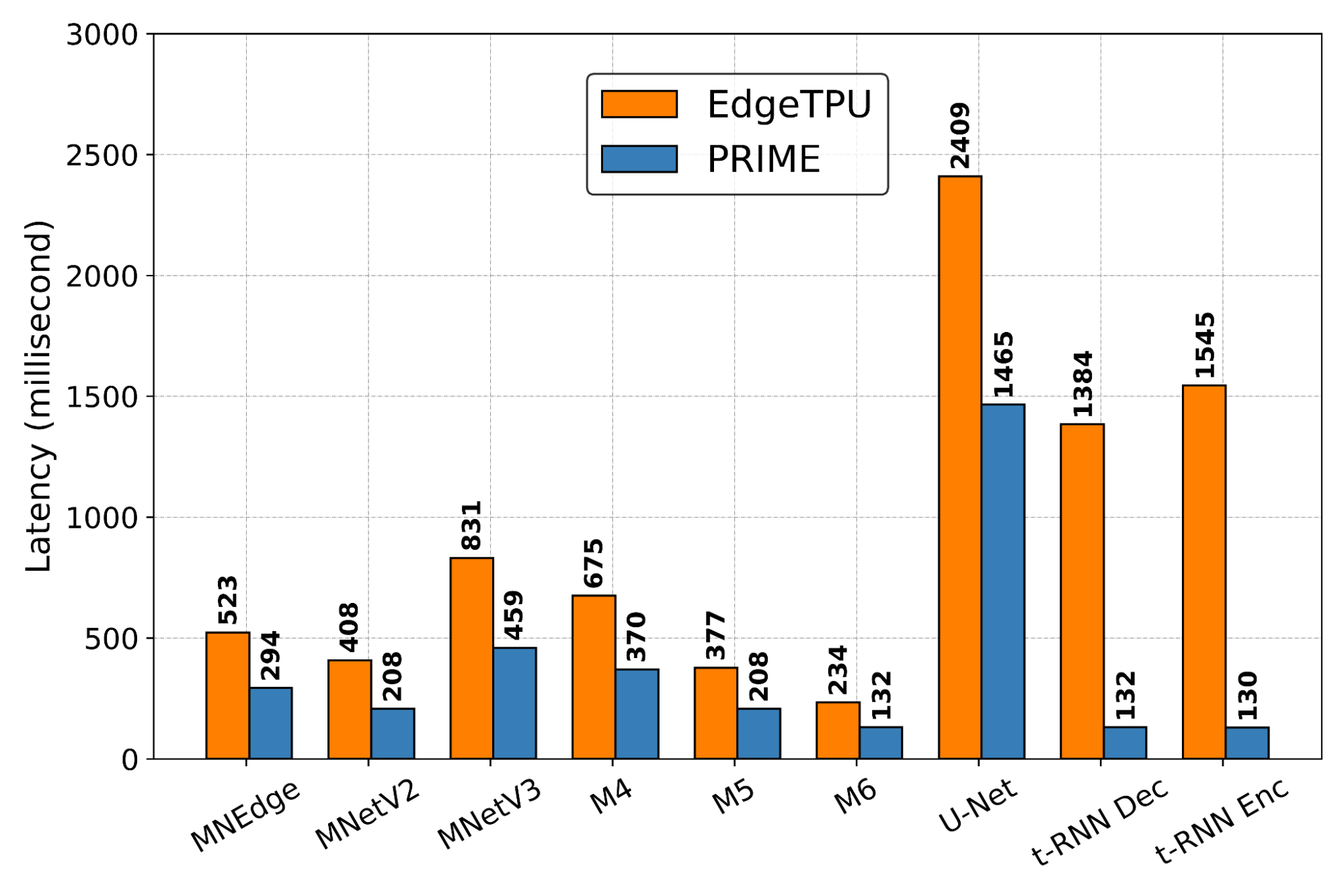
Comparing latencies (lower is better) of accelerator designs suggested by PRIME and EdgeTPU for single-model specialization.
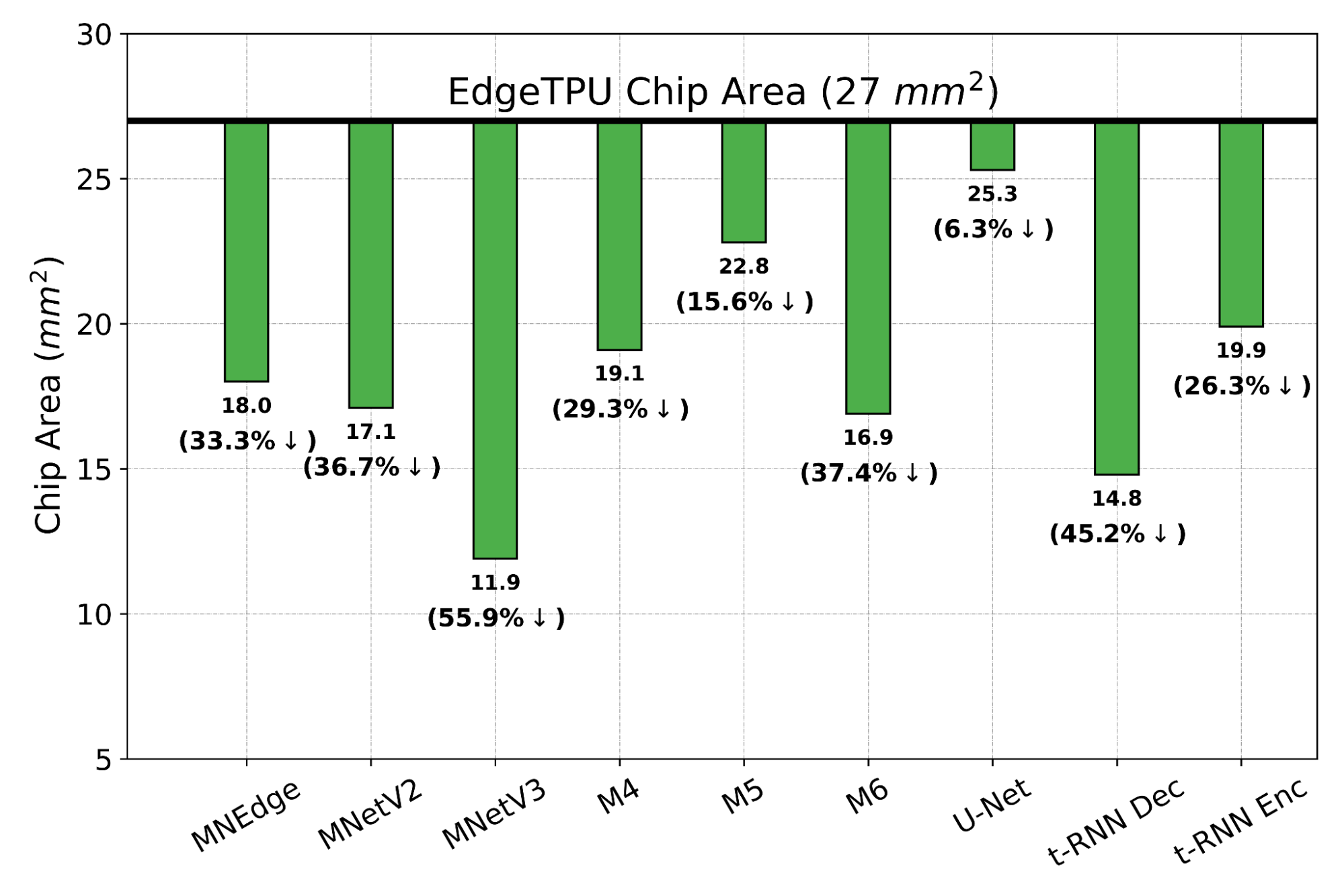
The chip area (lower is better) reduction compared to a baseline EdgeTPU design for single-model specialization.

Designing Accelerators for New and Multiple Applications, Zero-Shot
We now study how PRIME can use logged accelerator data to design accelerators for (1) multiple applications, where we optimize PRIME to design a single accelerator that works well across multiple applications simultaneously, and in a (2) zero-shot setting, where PRIME must generate an accelerator for new unseen application(s) without training on any data from such applications. In both settings, we train the contextual version of PRIME, conditioned on context vectors identifying the target applications and then optimize the learned model to obtain the final accelerator. We find that PRIME outperforms the best simulator-driven approach in both settings, even when very limited data is provided for training for a given application but many applications are available. Specifically in the zero-shot setting, PRIME outperforms the best simulator-driven method we compared to, attaining a reduction of 1.26x in latency. Further, the difference in performance increases as the number of training applications increases.

The average latency (lower is better) of test applications under zero-shot setting compared to a state-of-the-art simulator-driven approach. The text on top of each bar shows the set of training applications.

Closely Analyzing an Accelerator Designed by PRIME
To provide more insight to hardware architecture, we examine the best accelerator designed by PRIME and compare it to the best accelerator found by the simulator-driven approach. We consider the setting where we need to jointly optimize the accelerator for all nine applications, MobileNetEdge, MobileNetV2, MobileNetV3, M4, M5, M64, t-RNN Dec, and t-RNN Enc, and U-Net, under a chip area constraint of 100 mm2. We find that PRIME improves latency by 1.35x over the simulator-driven approach.

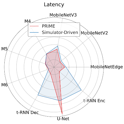
Per application latency (lower is better) for the best accelerator design suggested by PRIME and state-of-the-art simulator-driven approach for a multi-task accelerator design. PRIME reduces the average latency across all nine applications by 1.35x over the simulator-driven method.

As shown above, while the latency of the accelerator designed by PRIME for MobileNetEdge, MobileNetV2, MobileNetV3, M4, t-RNN Dec, and t-RNN Enc are better, the accelerator found by the simulation-driven approach yields a lower latency in M5, M6, and U-Net. By closely inspecting the accelerator configurations, we find that PRIME trades compute (64 cores for PRIME vs. 128 cores for the simulator-driven approach) for larger Processing Element (PE) memory size (2,097,152 bytes vs. 1,048,576 bytes). These results show that PRIME favors PE memory size to accommodate the larger memory requirements in t-RNN Dec and t-RNN Enc, where large reductions in latency were possible. Under a fixed area budget, favoring larger on-chip memory comes at the expense of lower compute power in the accelerator. This reduction in the accelerator's compute power leads to higher latency for the models with large numbers of compute operations, namely M5, M6, and U-Net.

Conclusion
The efficacy of PRIME highlights the potential for utilizing the logged offline data in an accelerator design pipeline. A likely avenue for future work is to scale this approach across an array of applications, where we expect to see larger gains because simulator-driven approaches would need to solve a complex optimization problem, akin to searching for needle in a haystack, whereas PRIME can benefit from generalization of the surrogate model. On the other hand, we would also note that PRIME outperforms prior simulator-driven methods we utilize and this makes it a promising candidate to be used within a simulator-driven method. More generally, training a strong offline optimization algorithm on offline datasets of low-performing designs can be a highly effective ingredient in at the very least, kickstarting hardware design, versus throwing out prior data. Finally, given the generality of PRIME, we hope to use it for hardware-software co-design, which exhibits a large search space but plenty of opportunity for generalization. We have also released both the code for training PRIME and the dataset of accelerators.

Acknowledgments
We thank our co-authors Sergey Levine, Kevin Swersky, and Milad Hashemi for their advice, thoughts and suggestions. We thank James Laudon, Cliff Young, Ravi Narayanaswami, Berkin Akin, Sheng-Chun Kao, Samira Khan, Suvinay Subramanian, Stella Aslibekyan, Christof Angermueller, and Olga Wichrowskafor for their help and support, and Sergey Levine for feedback on this blog post. In addition, we would like to extend our gratitude to the members of “Learn to Design Accelerators”, “EdgeTPU”, and the Vizier team for providing invaluable feedback and suggestions. We would also like to thank Tom Small for the animated figure used in this post.


1The infeasible accelerator designs stem from build errors in silicon or compilation/mapping failures. 
2This is akin to adversarial examples in supervised learning – these examples are close to the data points observed in the training dataset, but are misclassified by the classifier. 
3The performance metrics for the baseline EdgeTPU accelerator are extracted from an industry-based hardware simulator tuned to match the performance of the actual hardware. 
4These are proprietary object-detection models, and we refer to them as M4 (indicating Model 4), M5, and M6 in the paper. 

Source: Google AI Blog


An Open Source Vibrotactile Haptics Platform for On-Body Applications.

Most wearable smart devices and mobile phones have the means to communicate with the user through tactile feedback, enabling applications from simple notifications to sensory substitution for accessibility. Typically, they accomplish this using vibrotactile actuators, which are small electric vibration motors. However, designing a haptic system that is well-targeted and effective for a given task requires experimentation with the number of actuators and their locations in the device, yet most practical applications require standalone on-body devices and integration into small form factors. This combination of factors can be difficult to address outside of a laboratory as integrating these systems can be quite time-consuming and often requires a high level of expertise.

A typical lab setup on the left and the VHP board on the right.

In “VHP: Vibrotactile Haptics Platform for On-body Applications”, presented at ACM UIST 2021, we develop a low-power miniature electronics board that can drive up to 12 independent channels of haptic signals with arbitrary waveforms. The VHP electronics board can be battery-powered, and integrated into wearable devices and small gadgets. It allows all-day wear, has low latency, battery life between 3 and 25 hours, and can run 12 actuators simultaneously. We show that VHP can be used in bracelet, sleeve, and phone-case form factors. The bracelet was programmed with an audio-to-tactile interface to aid lipreading and remained functional when worn for multiple months by developers. To facilitate greater progress in the field of wearable multi-channel haptics with the necessary tools for their design, implementation, and experimentation, we are releasing the hardware design and software for the VHP system via GitHub.

Front and back sides of the VHP circuit board.
Block diagram of the system.

Platform Specifications.
VHP consists of a custom designed circuit board, where the main components are the microcontroller and haptic amplifier, which converts microcontroller’s digital output into signals that drive the actuators. The haptic actuators can be controlled by signals arriving via serial, USB, and Bluetooth Low Energy (BLE), as well as onboard microphones, using an nRF52840 microcontroller, which was chosen because it offers many input and output options and BLE, all in a small package. We added several sensors into the board to provide more experimental flexibility: an on-board digital microphone, an analog microphone amplifier, and an accelerometer. The firmware is a portable C/C++ library that works in the Arduino ecosystem.

To allow for rapid iteration during development, the interface between the board and actuators is critical. The 12 tactile signals’ wiring have to be quick to set up in order to allow for such development, while being flexible and robust to stand up to prolonged use. For the interface, we use a 24-pin FPC (flexible printed circuit) connector on the VHP. We support interfacing to the actuators in two ways: with a custom flexible circuit board and with a rigid breakout board.

VHP board (small board on the right) connected to three different types of tactile actuators via rigid breakout board (large board on the left).

Using Haptic Actuators as Sensors
In our previous blog post, we explored how back-EMF in a haptic actuator could be used for sensing and demonstrated a variety of useful applications. Instead of using back-EMF sensing in the VHP system, we measure the electrical current that drives each vibrotactile actuator and use the current load as the sensing mechanism. Unlike back-EMF sensing, this current-sensing approach allows simultaneous sensing and actuation, while minimizing the additional space needed on the board.

One challenge with the current-sensing approach is that there is a wide variety of vibrotactile actuators, each of which may behave differently and need different presets. In addition, because different actuators can be added and removed during prototyping with the adapter board, it would be useful if the VHP were able to identify the actuator automatically. This would improve the speed of prototyping and make the system more novice-friendly.

To explore this possibility, we collected current-load data from three off-the-shelf haptic actuators and trained a simple support vector machine classifier to recognize the difference in the signal pattern between actuators. The test accuracy was 100% for classifying the three actuators, indicating that each actuator has a very distinct response.

Different actuators have a different current signature during a frequency sweep, thus allowing for automatic identification.

Additionally, vibrotactile actuators require proper contact with the skin for consistent control over stimulation. Thus, the device should measure skin contact and either provide an alert or self-adjust if it is not loaded correctly. To test whether a skin contact measuring technique works in practice, we measured the current load on actuators in a bracelet as it was tightened and loosened around the wrist. As the bracelet strap is tightened, the contact pressure between the skin and the actuator increases and the current required to drive the actuator signal increases commensurately.

Current load sensing is responding to touch, while the actuator is driven at 250 Hz frequency.

Quality of the fit of the bracelet is measured.

Audio-to-Tactile Feedback
To demonstrate the utility of the VHP platform, we used it to develop an audio-to-tactile feedback device to help with lipreading. Lipreading can be difficult for many speech sounds that look similar (visemes), such as “pin” and “min”. In order to help the user differentiate visemes like these, we attach a microphone to the VHP system, which can then pick up the speech sounds and translate the audio to vibrations on the wrist. For audio-to-tactile translation, we used our previously developed algorithms for real-time audio-to-tactile conversion, available via GitHub. Briefly, audio filters are paired with neural networks to recognize certain viesemes (e.g., picking up the hard consonant “p” in “pin”), and are then translated to vibrations in different parts of the bracelet. Our approach is inspired by tactile phonemic sleeve (TAPS), however the major difference is that in our approach the tactile signal is presented continuously and in real-time.

One of the developers who employs lipreading in daily life wore the bracelet daily for several months and found it to give better information to facilitate lipreading than previous devices, allowing improved understanding of lipreading visemes with the bracelet versus lipreading alone. In the future, we plan to conduct full-scale experiments with multiple users wearing the device for an extended time.

Left: Audio-to-tactile sleeve. Middle: Audio-to-tactile bracelet. Right: One of our developers tests out the bracelets, which are worn on both arms.

Potential Applications
The VHP platform enables rapid experimentation and prototyping that can be used to develop techniques for a variety of applications. For example:

  • Rich haptics on small devices: Expanding the number of actuators on mobile phones, which typically only have one or two, could be useful to provide additional tactile information. This is especially useful as fingers are sensitive to vibrations. We demonstrated a prototype mobile phone case with eight vibrotactile actuators. This could be used to provide rich notifications and enhance effects in a mobile game or when watching a video.
  • Lab psychophysical experiments: Because VHP can be easily set up to send and receive haptic signals in real time, e.g., from a Jupyter notebook, it could be used to perform real-time haptic experiments.
  • Notifications and alerts: The wearable VHP could be used to provide haptic notifications from other devices, e.g., alerting if someone is at the door, and could even communicate distinguishable alerts through use of multiple actuators.
  • Sensory substitution: Besides the lipreading assistance example above, there are many other potential applications for accessibility using sensory substitution, such as visual-to-tactile sensing or even sensing magnetic fields.
  • Loading sensing: The ability to sense from the haptic actuator current load is unique to our platform, and enables a variety of features, such as pressure sensing or automatically adjusting actuator output.
Integrating eight voice coils into a phone case. We used loading sensing to understand which voice coils are being touched.

What's next?
We hope that others can utilize the platform to build a diverse set of applications. If you are interested and have ideas about using our platform or want to receive updates, please fill out this form. We hope that with this platform, we can help democratize the use of haptics and inspire a more widespread use of tactile devices.

Acknowledgments
This work was done by Artem Dementyev, Pascal Getreuer, Dimitri Kanevsky, Malcolm Slaney and Richard Lyon. We thank Alex Olwal, Thad Starner, Hong Tan, Charlotte Reed, Sarah Sterman for valuable feedback and discussion on the paper. Yuhui Zhao, Dmitrii Votintcev, Chet Gnegy, Whitney Bai and Sagar Savla for feedback on the design and engineering.

Source: Google AI Blog


Enhanced Sleep Sensing in Nest Hub

Earlier this year, we launched Contactless Sleep Sensing in Nest Hub, an opt-in feature that can help users better understand their sleep patterns and nighttime wellness. While some of the most critical sleep insights can be derived from a person’s overall schedule and duration of sleep, that alone does not tell the complete story. The human brain has special neurocircuitry to coordinate sleep cycles — transitions between deep, light, and rapid eye movement (REM) stages of sleep — vital not only for physical and emotional wellbeing, but also for optimal physical and cognitive performance. Combining such sleep staging information with disturbance events can help you better understand what’s happening while you’re sleeping.

Today we announced enhancements to Sleep Sensing that provide deeper sleep insights. While not intended for medical purposes1, these enhancements allow better understanding of sleep through sleep stages and the separation of the user’s coughs and snores from other sounds in the room. Here we describe how we developed these novel technologies, through transfer learning techniques to estimate sleep stages and sensor fusion of radar and microphone signals to disambiguate the source of sleep disturbances.

To help people understand their sleep patterns, Nest Hub displays a hypnogram, plotting the user’s sleep stages over the course of a sleep session. Potential sound disturbances during sleep will now include “Other sounds” in the timeline to separate the user’s coughs and snores from other sound disturbances detected from sources in the room outside of the calibrated sleeping area.

Training and Evaluating the Sleep Staging Classification Model
Most people cycle through sleep stages 4-6 times a night, about every 80-120 minutes, sometimes with a brief awakening between cycles. Recognizing the value for users to understand their sleep stages, we have extended Nest Hub’s sleep-wake algorithms using Soli to distinguish between light, deep, and REM sleep. We employed a design that is generally similar to Nest Hub’s original sleep detection algorithm: sliding windows of raw radar samples are processed to produce spectrogram features, and these are continuously fed into a Tensorflow Lite model. The key difference is that this new model was trained to predict sleep stages rather than simple sleep-wake status, and thus required new data and a more sophisticated training process.

In order to assemble a rich and diverse dataset suitable for training high-performing ML models, we leveraged existing non-radar datasets and applied transfer learning techniques to train the model. The gold standard for identifying sleep stages is polysomnography (PSG), which employs an array of wearable sensors to monitor a number of body functions during sleep, such as brain activity, heartbeat, respiration, eye movement, and motion. These signals can then be interpreted by trained sleep technologists to determine sleep stages.

To develop our model, we used publicly available data from the Sleep Heart Health Study (SHHS) and Multi-ethnic Study of Atherosclerosis (MESA) studies with over 10,000 sessions of raw PSG sensor data with corresponding sleep staging ground-truth labels, from the National Sleep Research Resource. The thoracic respiratory inductance plethysmography (RIP) sensor data within these PSG datasets is collected through a strap worn around the patient’s chest to measure motion due to breathing. While this is a very different sensing modality from radar, both RIP and radar provide signals that can be used to characterize a participant’s breathing and movement. This similarity between the two domains makes it possible to leverage a plethysmography-based model and adapt it to work with radar.

To do so, we first computed spectrograms from the RIP time series signals and used these as features to train a convolutional neural network (CNN) to predict the groundtruth sleep stages. This model successfully learned to identify breathing and motion patterns in the RIP signal that could be used to distinguish between different sleep stages. This indicated to us that the same should also be possible when using radar-based signals.

To test the generality of this model, we substituted similar spectrogram features computed from Nest Hub’s Soli sensor and evaluated how well the model was able to generalize to a different sensing modality. As expected, the model trained to predict sleep stages from a plethysmograph sensor was much less accurate when given radar sensor data instead. However, the model still performed much better than chance, which demonstrated that it had learned features that were relevant across both domains.

To improve on this, we collected a smaller secondary dataset of radar sensor data with corresponding PSG-based groundtruth labels, and then used a portion of this dataset to fine-tune the weights of the initial model. This smaller amount of additional training data allowed the model to adapt the original features it had learned from plethysmography-based sleep staging and successfully generalize them to our domain. When evaluated on an unseen test set of new radar data, we found the fine-tuned model produced sleep staging results comparable to that of other consumer sleep trackers.

The custom ML model efficiently processes a continuous stream of 3D radar tensors (as shown in the spectrogram at the top of the figure) to automatically compute probabilities of each sleep stage — REM, light, and deep — or detect if the user is awake or restless.

More Intelligent Audio Sensing Through Audio Source Separation
Soli-based sleep tracking gives users a convenient and reliable way to see how much sleep they are getting and when sleep disruptions occur. However, to understand and improve their sleep, users also need to understand why their sleep may be disrupted. We’ve previously discussed how Nest Hub can help monitor coughing and snoring, frequent sources of sleep disturbances of which people are often unaware. To provide deeper insight into these disturbances, it is important to understand if the snores and coughs detected are your own.

The original algorithms on Nest Hub used an on-device, CNN-based detector to process Nest Hub’s microphone signal and detect coughing or snoring events, but this audio-only approach did not attempt to distinguish from where a sound originated. Combining audio sensing with Soli-based motion and breathing cues, we updated our algorithms to separate sleep disturbances from the user-specified sleeping area versus other sources in the room. For example, when the primary user is snoring, the snoring in the audio signal will correspond closely with the inhalations and exhalations detected by Nest Hub’s radar sensor. Conversely, when snoring is detected outside the calibrated sleeping area, the two signals will vary independently. When Nest Hub detects coughing or snoring but determines that there is insufficient correlation between the audio and motion features, it will exclude these events from the user’s coughing or snoring timeline and instead note them as “Other sounds” on Nest Hub’s display. The updated model continues to use entirely on-device audio processing with privacy-preserving analysis, with no raw audio data sent to Google’s servers. A user can then opt to save the outputs of the processing (sound occurrences, such as the number of coughs and snore minutes) in Google Fit, in order to view their night time wellness over time.

Snoring sounds that are synchronized with the user’s breathing pattern (left) will be displayed in the user’s Nest Hub’s Snoring timeline. Snoring sounds that do not align with the user’s breathing pattern (right) will be displayed in Nest Hub’s “Other sounds” timeline.

Since Nest Hub with Sleep Sensing launched, researchers have expressed interest in investigational studies using Nest Hub’s digital quantification of nighttime cough. For example, a small feasibility study supported by the Cystic Fibrosis Foundation2 is currently underway to evaluate the feasibility of measuring night time cough using Nest Hub in families of children with cystic fibrosis (CF), a rare inherited disease, which can result in a chronic cough due to mucus in the lungs. Researchers are exploring if quantifying cough at night could be a proxy for monitoring response to treatment.

Conclusion
Based on privacy-preserving radar and audio signals, these improved sleep staging and audio sensing features on Nest Hub provide deeper insights that we hope will help users translate their night time wellness into actionable improvements for their overall wellbeing.

Acknowledgements
This work involved collaborative efforts from a multidisciplinary team of software engineers, researchers, clinicians, and cross-functional contributors. Special thanks to Dr. Logan Schneider, a sleep neurologist whose clinical expertise and contributions were invaluable to continuously guide this research. In addition to the authors, key contributors to this research include Anupam Pathak, Jeffrey Yu, Arno Charton, Jian Cui, Sinan Hersek, Jonathan Hsu, Andi Janti, Linda Lei, Shao-Po Ma, ‎Jo Schaeffer, Neil Smith, Siddhant Swaroop, Bhavana Koka, Dr. Jim Taylor, and the extended team. Thanks to Mark Malhotra and Shwetak Patel for their ongoing leadership, as well as the Nest, Fit, and Assistant teams we collaborated with to build and validate these enhancements to Sleep Sensing on Nest Hub.


1Not intended to diagnose, cure, mitigate, prevent or treat any disease or condition. 
2Google did not have any role in study design, execution, or funding. 

Source: Google AI Blog


Open source SystemVerilog tools in ASIC design

Open source hardware is undeniably undergoing a renaissance whose origin can be traced to the establishment of RISC-V Foundation (later redubbed RISC-V International). The open ISA and ecosystem, in which Antmicro participated since the beginning as a Founding member, has sparked many open source CPU implementations, new tooling, methodologies, and trends which allow for more collaborative and software driven design.

Many of those broader open hardware activities have been finding a home in CHIPS Alliance, an open source organization we participate in as a Platinum member alongside Google, Intel, Western Digital, SiFive and others, whose goals explicitly encompass:
  • creating and maintaining open source ASIC and FPGA design tools (digital and analog)
  • open source core and uncore IP
  • interconnects, interoperability specs and more
This is in perfect alignment with Antmicro’s mission—as we’ve been heavily involved with many of the projects inside of and related to CHIPS providing commercial support, engineering services, and assistance in practical adoption for enterprise deployments.

As of this time, a range of everyday design, development, testing, and verification tasks are already possible using open source tools and components and are part of our and our customer’s everyday workflow. Other developments are within reach given a reasonable amount of development, which we can provide based on specific scenarios. Others still are much further away, but with dedicated efforts inside CHIPS in which we are involved together with partners like Google and Western Digital, there is a pathway towards a completely open hardware design and verification ecosystem. This will eventually unlock incredible potential in new design methodologies, vertical integration capabilities, and education and business opportunities. Until then, Antmicro can help you with extracting practical value for many scenarios such as simulation, linting, formatting, synthesis, continuous integration and more.

Building a SystemVerilog ecosystem in CHIPS

Some of the challenges towards practical adoption of open source in ASIC design have been related to the fact that a significant proportion of advanced ASIC design is done in SystemVerilog, a fairly complex and powerful language in its own right, which used to be poorly supported in the open source tooling ecosystem. Partial solutions like SystemVerilog to Verilog converters or paid plugins existed, but direct support lagged behind, making open source tools for SystemVerilog a difficult sell previously.

This has been fortunately changing rapidly with a dedicated development effort spearheaded by Google and Antmicro. Projects in this space include Verible, Surelog, UHDM and sv-tests that we have been developing, as well as integrating with existing tools like Yosys, Verilator under the umbrella of the SymbiFlow open source FPGA project, and which are now officially being transferred into the CHIPS Alliance to increase awareness and build a broader SystemVerilog ecosystem.

In this note, we will walk you through the state of the art in new SystemVerilog capabilities in open source projects, and invite you to reach out to see how CHIPS Alliance’s SystemVerilog projects can be useful to you today or in the near future.

A walk through the state of the art in new SystemVerilog capabilities in open source projects

Verible

The Verible project originated at Google; its main mission is to make SystemVerilog easily and quickly parsable for a wide variety of applications mostly focusing on developer tools.

Verible is a set of tools based on a common SystemVerilog parsing engine, providing a command line interface which makes integration with other tools for daily usage or CI systems for automatic testing and deployment a breeze.

Antmicro has been involved in the development of Verible since its initial open source release and we now provide a significant portion of current development efforts, helping adapt it for use in various open source projects or commercial environments that use SystemVerilog. One notable user is the security-focused OpenTitan project, which has driven many interesting developments and provides a good showcase of the capabilities being completely open source, well documented, fairly complex, and used in real applications.

Linter

One of the most common use cases for Verible is linting. The linter analyzes code for patterns and constructs that are deemed undesirable according to the implemented lint rules. The rules follow authoritative style guides that can be enforced on a project or company level in various SystemVerilog projects.

The rules range from simple ones like making sure the module name matches the file name to more sophisticated like checking variable naming conventions (all caps, snake case, specific prefix or suffix etc.) or making sure the labels after the begin and end statements match.

A full list of rules can be found in the Verible lint documentation and is constantly growing. Usage is very simple:

$ verible-verilog-lint --ruleset all core.sv 

core.sv:3:11: Interface names must use lower_snake_case naming convention and end with _if. [Style: interface-conventions] [interface-name-style]


The output of the linter is easy to understand, as the way issues are reported to the user is modeled after popular programming language compilers.

The linter is highly configurable. It is possible to select the rules for which the compliance will be checked, some rules allow for detailed configuration (e.g. max line length).

Rules can also be selectively waived in specific files or at specific lines or even by regex matching. In addition, some rules can be automatically fixed by the linter itself.

Formatter

The Verible formatter is a complementary tool for the linter. It is used to automatically detect various formatting issues like improper indentation or alignment. As opposed to the linter, it only detects and fixes issues that have no lexical impact on the source code.

The formatter also comes with useful helper scripts for selective and interactive reformatting (e.g. only format files that changed according to git, ask before applying changes to each chunk).

A toolset that consists of both the linter and the formatter can effectively remove all the discussions about styling, preferences and conventions from all pull requests. Developers can then focus solely on the technical aspects of the proposed changes.

$ cat sample.sv

typedef struct {

bit first;

        bit second;

bit

   third

        ;

  bit fourth;

bit fifth; bit sixth;

}

 foo_t;


$ verible-verilog-format sample.sv

typedef struct {

  bit first;

  bit second;

  bit third;

  bit fourth;

  bit fifth;

  bit sixth;

} foo_t;

Indexer

The Verible parser itself can be relatively easily used to perform many other tasks. One of the interesting use cases is generating a Kythe compatible indexing database.

Indexing a SystemVerilog project makes it very easy to collaborate on a project remotely. It is possible to navigate through the source code using nothing else than just a web browser.

The Kythe integration can be served on an arbitrary server, can be deployed after every commit in a project, etc. A showcase of the indexing mechanism can be found in our GitHub repository. The demo downloads the latest version of the Ibex core, indexes it, and deploys it to be viewed on a remote machine. The results can be viewed on the example index webpage.

The demo downloads the latest version of the Ibex core, indexes it, and deploys it to be viewed on a remote machine. The results can be viewed on the example index webpage.

Indexing is widely adopted for many larger open source software projects.

Thanks to Verible, it is now possible to do the same in the world of open source HDL designs, and of course private, company-wide deployments like this are also possible.

Surelog and UHDM

SystemVerilog is a powerful language but also complex. So far no open source tools have been able to support it in full. Implementing it separately for each project such as the Yosys synthesis tool or the Verilator simulator would take a colossal amount of time, and that’s where Surelog and UHDM come in.

Surelog, originally created and led by Alain Dargelas, aims to be a fully-featured SystemVerilog 2017 preprocessor, parser, and elaborator. It’s a modern tool and thus follows the current version of the SV standard without unnecessary deviations or legacy baggage.

What’s interesting is that Surelog is only a language frontend designed to integrate well with other tools—it outputs an elaborated design in an intermediate format called UHDM.

UHDM stands for Universal Hardware Data Model, and it’s both a file format for storing hardware designs and a library able to manipulate this format. A client application can access the data using VPI, which is a standard programming interface for SystemVerilog.

What this means is that the work required to create a SystemVerilog parser only needs to be done once, and other tools can use that parser via UHDM. This is much easier than implementing a full SystemVerilog parser within each tool. What’s more, any improvements in the unified parser will provide benefits for all client applications. Finally, any other parser is free to emit UHDM as well, so in the future we might see e.g. a UHDM backend for Verible.

Just like in Verible’s case, both Surelog and UHDM have recently been contributed into CHIPS Alliance to drive a broader adoption. We are actively contributing to both projects, especially around the integrations with tooling such as Yosys and Verilator, and practical use in open source and customer projects.

Recent Antmicro contributions adding UHDM frontends for Yosys and Verilator enabled Ibex synthesis and simulation. The complete OpenTitan project is the next milestone.

The Surelog/UHDM/Yosys flow enabling SystemVerilog synthesis without the necessity of converting the HDL code to Verilog is a great improvement for open source ASIC build flows such as OpenROAD’s OpenLane flow (which we also support commercially). Removing the code conversion step enables the developers to perform e.g. circuit equivalence validation to check the correctness of the design.

More information about Surelog/UHDM and Verible can be found in a dedicated CHIPS Alliance presentation that was recently given by Henner Zeller, Google’s Verible lead.

UVM is in the picture

No open source ASIC design toolkit can be complete without support for Universal Verification Methodology, or UVM, which is one of the most widespread verification methodologies for large-scale ASIC design. This has also been an underrepresented area in open source tooling and changing that is an enormous undertaking, but working together with our customers, most notably Western Digital, we have been making progress on that front as well.

Across the ASIC development landscape, UVM verification is currently performed with proprietary simulators, but a more easily distributable, collaborative and open ecosystem is needed to close the feedback loop between (emerging) open source design approaches and verification. Verilator is an extremely popular choice for other system development use cases but it has historically not focused on UVM-style verification. Other styles of verification, such as the very interesting and popular Python-based cocotb framework maintained by FOSSi Foundation, have been enabled in Verilator. But support for UVM, partly due to the size and complexity of the methodology, has been notably absent.

One of the features missing from Verilator but needed for UVM is SystemVerilog stratified scheduling, which is a set of rules specified in the standard that govern the way time progresses in a simulation, as well as the order of operations. A SystemVerilog simulation is divided into smaller steps called time slots, and each time slot is further divided into multiple regions. Specific events can only happen in certain regions, and some regions can reoccur in a single time slot.

Until recently, Verilator had implemented only a small subset of these rules, as all scheduling was being done at compilation time. Spearheading a long-standing development effort within CHIPS Alliance, in collaboration with the maintainer of Verilator, Wilson Snyder, we have built is a proof-of-concept version of Verilator with a dynamic scheduler, which manages the occurrence of certain events at runtime, extending the stratified scheduling support. More details can be found in Antmicro’s presentation for the inaugural CHIPS Alliance Deep Dive Cafe Talk.

Another feature required for UVM is constrained randomization, which allows generating random inputs to feed to a design in order to thoroughly test it. Unlike unconstrained randomization, which is already provided by Verilator, it allows the user to specify some rules for input generation, thus limiting the possible value space and making sure that the input makes sense. Work on adding this to Verilator has already started, although the feature is still in its infancy. There are many other features on the roadmap which will eventually enable practical UVM support—stay tuned with our CHIPS Alliance events to follow that development.

What next?

Support for SystemVerilog parsers, for the intermediate format, and for their respective backends and integrations with various tooling, as well as for UVM is now under heavy development. If you would like to see more effort put into a specific area, reach out to us at [email protected]. Antmicro offers commercial support services to extend the flows we’ve briefly presented here to various practical applications and designs, and to effectively integrate this approach into people’s workflows.

Adding to this our cloud expertise, Antmicro customers can benefit from a complete and industry-proven methodology scalable between teams and across on-premise and cloud installations, transforming chip design workflows to be more software-driven and collaborative. To take advantage of open source solutions with tools like Verilator, Yosys, OpenROAD and others - tell us about your use case and we will see what can be done today.

If you are interested in collaborating on the development of SystemVerilog-focused and other open hardware tooling, join CHIPS Alliance and participate in our workgroups and help us push innovation in ASIC design forward.

Originally posted on the Antmicro blog.

By guest author Michael Gielda, Antmicro, and Tim Ansell, Software Engineer