
With malicious software on the rise, how can you be certain that a computer, server, or mobile device is running the code (and provisioning data) that was intended? You can't just ask the code itself, so where do you start? The answer is deceptively simple – start where you have certainty and build up a chain of trust. For communication on the web, we rely on Certificate Authorities (CAs) to ensure the security of web content before it reaches the user. In products composed of an interconnected jungle of hardware and software, like Chromebooks and our Cloud infrastructure, we rely on a small dedicated secure microcontroller called a Root of Trust (RoT). And, some devices even have several RoTs for specialized needs.
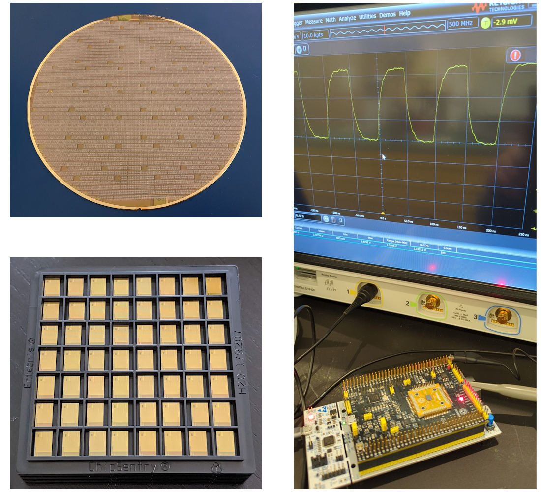
Over the past six years, Google has been working with the open source community to build OpenTitan, the first open source silicon RoT. Today, we are excited to announce that we have started fabrication of the first production-ready OpenTitan silicon by Nuvoton. This silicon will be the first broadly used RoT chip at Google with a fully transparent design and origin. We have production OpenTitan chips available for lab testing and evaluation with larger volumes available from Nuvoton starting in Spring 2025.
 |
History of RoTs and OpenTitan at Google
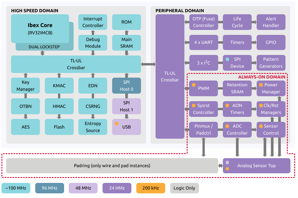
In 2009, Google began shipping devices with dedicated off-the-shelf RoTs. By 2014, it became clear that higher levels of assurance would only be attainable by investing in a first party RoT solution. A first party solution enabled Google to have full visibility and control over the security of its products throughout their life cycles. Previous off-the-shelf parts were black- or gray-box solutions where vendors are responsible for designing their own hardware and software – all with limited or no access to the source. Without full transparency, it is impossible to completely understand the security assurances for products using these proprietary parts. In addition, it was becoming harder to meet product needs with off-the-shelf RoT solutions, from footprint to function to cost – we needed a better solution for Chromebooks, Cloud, and later, Pixel.
Today, open source software powers nearly every consumer experience, from open source operating systems like Linux, to web browsers like Chromium. Open source is often the most economically efficient solution for developing foundational technology: it enables companies to work together and pool resources to build common, compatible products. Until now, this development approach has not been demonstrated in a commercially relevant setting for silicon.
OpenTitan is the first open-source silicon project to reach commercial availability based on the engineering samples we released last year. The OpenTitan project started from scratch in 2018 with a coalition of commercial, academic, and not-for-profit partners. The OpenTitan project is hosted by lowRISC CIC in Cambridge, UK. Google and project partners – Nuvoton, ETH Zurich, G+D Mobile Security, lowRISC, Rivos, Seagate, Western Digital, Winbond, zeroRISC, and a number of independent contributors – provide open source hardware register-transfer level (RTL) and design verification (DV) code, along with integration guidelines, and reference firmware to drive adoption throughout industry.
The Future
With the introduction of production-ready OpenTitan chips, we are excited to welcome an era where security is based on transparency from the very beginning of the stack. OpenTitan is the first commercially available open source RoT to support PQC secure boot based on SLH-DSA (formerly known as SPHINCS+). Our vision is that these chips will help drive broader industry adoption not only of open designs and their security properties, but also of this innovative method of open source collaboration between organizations.
Samples of production OpenTitan silicon are now available, with reference provisioning and application-level firmware releases coming soon. Product integrations have begun to intercept Chromebooks shipping later this year, with datacenter integrations following shortly after.
Getting Involved
With OpenTitan, we’ve introduced brand new methodologies for how commodity chips get designed that are increasingly economical moving forward. OpenTitan provides Google with a high-quality, low-cost, commoditized hardware RoT that can be used across the Google ecosystem. This will also facilitate the broader adoption of Google-endorsed security features across the industry.
The fabrication of production OpenTitan silicon is the realization of many years of dedication and hard work from our team. It is a significant moment for us and all contributors to the project. OpenTitan’s broad community has been critical to its success. As the following metrics show (baselined from the project’s public launch in 2019), the OpenTitan community is rapidly growing:
- Almost nine times the number of commits at launch: from 2,500 to over 24,200.
- 176 contributors to the code base
- 17k+ merged pull requests
- 1.5M+ LoC, including 500k LoC of HDL
- 2.5k Github stars
If you are interested in learning more or contributing to OpenTitan, visit the open source GitHub repository or reach out to the OpenTitan team.
By