Over the last year we have been busy planning the expansion of our free open source silicon design and manufacturing program to further grow the community of developers and companies building custom silicon, and build a thriving ecosystem around open source hardware.
Today, we’re excited to announce an expansion of this program and our partnership with GlobalFoundries. Together, we're releasing the Process Design Kit (PDK) for the GlobalFoundries 180MCU technology platform under the Apache 2.0 license, along with a no-cost silicon realization program to manufacture open source designs on the Efabless platform. This open source PDK is the first result of our ongoing partnership with GF. Based on the scale and breadth of GF’s technology and manufacturing expertise, we expect to do more together to further access and innovation in semiconductor development and manufacturing.
 |
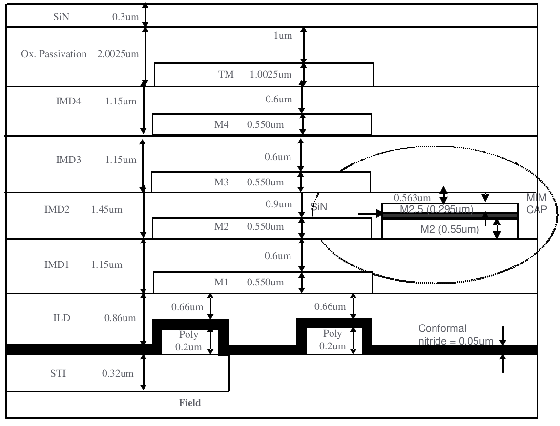
GF180MCU 1P5M 5 metals stack-up, 9kA top metal, with MIM between M3 and M4 layers. |
Over the past few years, the world has experienced an unprecedented acceleration of adoption of digital capabilities—driven by the pandemic, and technology megatrends that have shifted every aspect of human life. According to GlobalFoundries, this has led to roughly 73% of foundry revenue being associated with high growth markets such as mobile, IoT, and automotive. This transition has not only given rise to a “New Golden Age” of semiconductors but also a tectonic shift in how we define and deliver innovation as an industry.
Specifically, applications using 180nm are at a global capacity of 16+ million wafers a year and bound to grow to 22+ million wafers in 2026, according to GlobalFoundries.
The 180nm application space continues to see strong market traction in motor controller, RFID, general purpose MCUs and PMIC, along with emerging applications such as IoT Sensors, Dual Frequency RFID and Motor Drive.
The collaboration between GlobalFoundries and Google will help drive innovation for the application and silicon engineers designing in these high growth areas, and is an unambiguous affirmation of the viability of the open source model for the foundry ecosystem.
The GF 180nm technology platform offers open source silicon designers new capabilities for high volume production, affordability, and more voltage options. This PDK includes the following standard cells
- Digital standard cells libraries (7-track and 9-track)
- Low (3.3V), Medium (5V, 6V) and High (10V) voltage devices
- SRAM macros (64x8, 128x8, 256x8, 512x8)
- I/O and primitives (Resistors, Capacitors, Transistors, eFuses) cells libraries
- Open source EDA tools can now add support for multiple process technologies.
- Researchers can produce fully-reproducible designs against multiple technology baselines.
- Popular open source IP blocks can be ported to different process technologies.
We encourage you to:
- visit developers.google.com/silicon,
- explore the GF180MCU PDK repository and documentation,
- and join the gf180mcu-pdk-users@ and gf180mcu-pdk-announce@ mailing lists to get notified about future OpenMPW shuttle opportunities that target this new technology!
By Johan Euphrosine and Ethan Mahintorabi – Hardware Toolchains Team

